
Publications
The majority of the Facility’s publications arise from the research undertaken on wafers by users. Publications on epitaxy developments itself often arise through our Pump Priming scheme. Publications are primarily in material science journals, and journals dedicated to device technologies. They are therefore widely read by the semiconductor community, and are also influential on industry evaluation of technologies.
- Publications are co-authored by NEF staff, or the NEF contribution is acknowledged by our users.
- Publications on epitaxy developments itself often arise through our Pump Priming scheme.
- Our Publications are primarily in Material Science journals and journals dedicated to device technologies which are widely read by the semiconductor community, and are also influential on industry evaluation of technologies.
View the full list of our III-V and Silicon Technology Publications from 2016-2025:
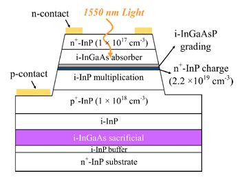
Micro-transfer printing of InGaAs/InP avalanche photodiode on Si substrate
We report on the fabrication and micro-transfer printing (µ-TP) of InGaAs/InP avalanche photodiodes (APDs) onto silicon substrates. A process flow was developed to suspend the devices using semiconductor tethers. The developed process reduces the number of fabrication steps required compared to methods based on the use of photoresist tethers. Furthermore, our process is compatible with devices that may be susceptible to damage induced by the photoresist removal process. APDs were characterised in linear mode operation both before suspension and after printing. Despite the additional fabrication steps required to suspend the APD membranes and the physical nature of the µ-TP process, the electrical characteristics of the devices were preserved. No degradation in the optical performance of the devices was measured. Our work represents the first demonstration of µ-TP of InGaAs/InP APDs onto silicon substrates. The results highlight the viability of µ-TP for effective heterogeneous integration of InGaAs/InP APDs with silicon photonic integrated circuits for optical and quantum communication and other light detection applications.
Read the full article here: Micro-transfer printing of InGaAs/InP avalanche photodiode on Si substrate
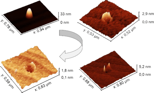
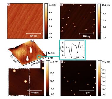
Local Droplet Etching with Indium Droplets on InP(100) by Metal-Organic Vapor Phase Epitaxy
The local droplet etching (LDE) by using indium droplets on bare InP(100) surfaces is demonstrated in a metal–organic vapor phase epitaxy (MOVPE) environment for the first time. The role of an arsenic flow applied to self-assembled metallic indium droplets is systematically studied. Increasing the arsenic supply leads to the formation of ring-like nanostructures and nanoholes. The results are analyzed with reference to LDE in a molecular beam epitaxy environment, where such a technique is well established, particularly for arsenide-based III–V semiconductors, and where only one group-V material is involved. Here, As–P exchange reactions at droplet sites are identified as the drivers for the formation of nanoholes. Such nanoholes can serve as nucleation sites for subsequent fabrication of highly symmetric QDs by nanohole-infilling or as a means for in situ surface nanopatterning. LDE on InP by MOVPE can thus be considered as a promising approach for the cost-effective fabrication of novel quantum emitters at the telecom C-band.
Read the full article here: Local Droplet Etching with Indium Droplets on InP(100) by Metal–Organic Vapor Phase Epitaxy
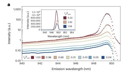
Bose–Einstein condensation of light in a semiconductor quantum well microcavity
When particles with integer spin accumulate at low temperature and high density, they undergo Bose–Einstein condensation (BEC). Atoms, magnons, solid-state excitons, surface plasmon polaritons and excitons coupled to light exhibit BEC, which results in high coherence due to massive occupation of the respective system’s ground state. Surprisingly, photons were shown to exhibit BEC recently in organic-dye-filled optical microcavities, which—owing to the photon’s low mass—occurs at room temperature. Here we demonstrate that photons within an inorganic semiconductor microcavity also thermalize and undergo BEC. Although semiconductor lasers are understood to operate out of thermal equilibrium, we identify a region of good thermalization in our system where we can clearly distinguish laser action from BEC. Semiconductor microcavities are a robust system for exploring the physics and applications of quantum statistical photon condensates. In practical terms, photon BECs offer their critical behaviour at lower thresholds than lasers. Our study shows two further advantages: the lack of dark electronic states in inorganic semiconductors allows these BECs to be sustained continuously; and quantum wells offer stronger photon–photon scattering. We measure an unoptimized interaction parameter (g???10–3), which is large enough to access the rich physics of interactions within BECs, such as superfluid light.
Read the full article here: Bose–Einstein condensation of light in a semiconductor quantum well microcavity
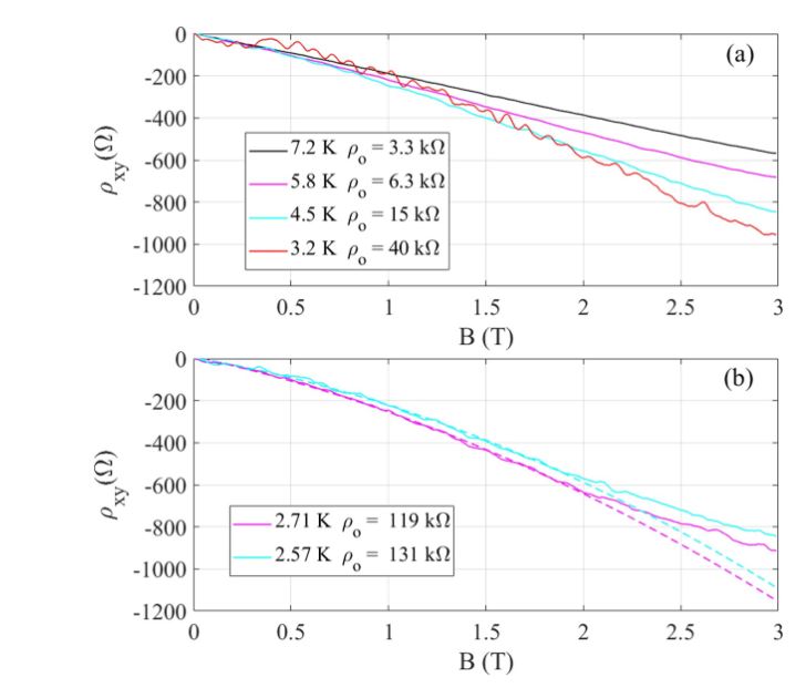
MBE growth of Ge1?x Snx devices with intrinsic disorder
We discuss the electrical properties of MBE (molecular beam epitaxy) grown, modulation doped, Ge1-xSnx quantum well devices. A consequence of the epitaxial growth process is that electronic disorder is introduced even in modulation doped quantum well structures and electrical transport properties that are characteristic of a high level of disorder are apparent. MBE growth of this material also results in the surface segregation of elemental ?-Sn in the way that has been observed utilizing other epitaxial growth methods. A thermally activated, p-type mobility is a clear feature of the electrical properties with generally temperature independent hole densities ~ 1012 cm-2 from the measured Hall effect and coming from the modulation doping. We present a discussion of Hall effect measurements in this disordered regime. The percolation carrier density in MBE modulation doped GeSn is in the region of ~ 1×1012 cm-2 although Hall measurements in this regime are difficult to quantify when the resistivity > (h/e2). In this notation h is Planck’s constant and e is the unit of charge. Conductivities (?) as low as ~ 0.028×(e2/h)×square can be measured in the 4-contact ac configuration and the temperature dependence indicates a mobility edge in these p-type devices below ~ 2×1012 cm-2. At lower temperatures (< ~1 K) the presence of a Coulomb gap can be determined using dc transport, constant voltage measurements where small ac current excitation is not available experimentally. This 2-contact configuration can determine ? down to ~ 10-6×(e2/h), deep into the localization regime, revealing a hopping conductivity dominated system. We discuss the relevance of these electrical properties for MBE grown GeSn devices.
Read the full article here: MBE growth of Ge1?x Snx devices with intrinsic disorder
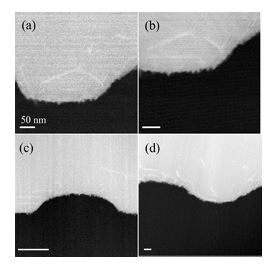
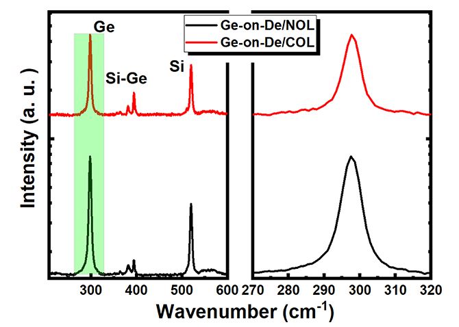
High-quality germanium growth on (111)-faceted V-groove silicon by molecular beam epitaxy
High-quality and low-defect-density germanium (Ge) buffer layers on silicon (Si) substrates have long been developed for group IV and III–V devices by suppressing defect propagation during epitaxial growth. This is a crucial step for the development of highly efficient photonic devices on Si substrates. Patterned silicon substrates have increasingly been employed for their ability to restrict and hinder the motion of defects. In this work, we demonstrate the effectiveness of an optimised two-step growth recipe structure on a (111)-faceted V-groove silicon substrate with a 350 nm flat ridge. This strategy successfully reduces the threading dislocation (TD) density while growing a 1 ?m Ge buffer layer via molecular beam epitaxy. As a result, a high-quality buffer is produced with a low TD density on the order of 107 cm?2 and a surface roughness below 1 nm.
Read the full article: High-quality germanium growth on (111)-faceted V-groove silicon by molecular beam epitaxy
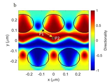
Topological and conventional nanophotonic waveguides for directional integrated quantum optics
Directionality in integrated quantum photonics has emerged as a promising route towards achieving scalable quantum technologies with nonlinearities at the single-photon level. Topological photonic waveguides have been proposed as a novel approach to harnessing such directional light-matter interactions on-chip. However, uncertainties remain regarding the strength of the directional coupling of embedded quantum emitters to topological waveguides in comparison to conventional line defect waveguides. In this work we present an investigation of directional coupling in a range of waveguides using a combination of experimental, theoretical, and numerical analyses. We quantitatively characterize the position dependence of the light-matter coupling on several topological photonic waveguides and benchmark their directional coupling performance against conventional line defect waveguides. We conclude that topological waveguides underperform in comparison to conventional line defect waveguides, casting their directional optics credentials into doubt. To demonstrate this is not a question of the maturity of the field; we show that state-of-the-art inverse design methods, while capable of improving the directional emission of these topological waveguides, still place them significantly behind the operation of a conventional (glide-plane) photonic crystal waveguide. Our results and conclusions pave the way towards improving the implementation of quantitatively predicted quantum nonlinear effects on-chip.
Read the full article here: Topological and conventional nanophotonic waveguides for directional integrated quantum optics
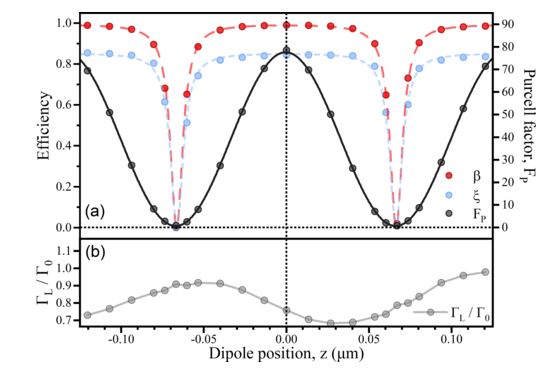
Probing Purcell enhancement and photon collection efficiency of InAs quantum dots at nodes of the cavity electric field.
The interaction of excitonic transitions with confined photonic modes enables tests of quantum physics and design of efficient optoelectronic devices. Here we study how key metrics such as Purcell factor, ? factor, and collection efficiency are determined by the non-cavity modes that exist in real devices, taking the well-studied micropillar cavity as an example. Samples with dots at different positions in the cavity field allow us to quantify the effect of the non-cavity modes and show that the zero-phonon line and the phonon-assisted emission into the cavity mode H?E11 is suppressed by positioning dots at the field node.
Read the full article here: Probing Purcell enhancement and photon collection efficiency of InAs quantum dots at nodes of the cavity electric field
Exploring the Implementation of GaAsBi Alloys as Strain-Reducing Layers in InAs/GaAs Quantum Dots
This paper investigates the effect of GaAsBi strain reduction layers (SRLs) on InAs QDs with different Bi fluxes to achieve nanostructures with improved temperature stability. The SRLs are grown at a lower temperature (370 • C) than the usual capping temperature for InAs QDs (510 • C). The study finds that GaAs capping at low temperatures reduces QD decomposition and leads to larger pyramidal dots but also increases the threading dislocation (TD) density. When adding Bi to the capping layer, a significant reduction in TD density is observed, but unexpected structural changes also occur. Increasing the Bi flux does not increase the Bi content but rather the layer thickness. The maximum Bi content for all layers is 2.4%. A higher Bi flux causes earlier Bi incorporation, along with the formation of an additional InGaAs layer above the GaAsBi layer due to In segregation from QD erosion. Additionally, the implementation of GaAsBi SRLs results in smaller dots due to enhanced QD decomposition, which is contrary to the expected function of an SRL. No droplets were detected on the surface of any sample, but we did observe regions of horizontal nanowires within the epilayers for the Bi-rich samples, indicating nanoparticle formation.
Read the full article: Exploring the Implementation of GaAsBi Alloys as Strain-Reducing Layers in InAs/GaAs Quantum Dots
Anomalous luminescence temperature dependence of (In,Ga)(As,Sb)/GaAs/GaP quantum dots overgrown by a thin GaSb capping layer for nanomemory applications
We study (In,Ga)(As,Sb)/GaAs quantum dots (QDs) embedded in a GaP (100) matrix, which are overgrown by a thin GaSb capping layer with variable thickness. QD samples are studied by temperature-dependent photoluminescence, and we observe that the QD emission shows anomalous temperature dependence, i.e. increase of energy with temperature increase from 10?K to ?70?K, followed by energy decrease for larger temperatures. With the help of fitting of luminescence spectra by Gaussian bands with energies extracted from eight band k?p theory with multiparticle corrections calculated using the configuration interaction method, we explain the anomalous temperature dependence as mixing of momentum direct and indirect exciton states. We also find that the k-indirect electron–hole transition in type-I regime at temperatures <70?K is optically more intense than k-direct. Furthermore, we identify a band alignment change from type-I to type-II for QDs overgrown by more than one monolayer of GaSb. Finally, we predict the retention time of (In,Ga)(As,Sb)/GaAs/AlP/GaP QDs capped with GaSb layers with varying thickness, for usage as storage units in the QD-Flash nanomemory concept and observe that by using only a 2?ML-thick GaSb capping layer, the projected storage time surpasses the non-volatility limit of ten years.
Read the full article here: Anomalous luminescence temperature dependence of (In,Ga)(As,Sb)/GaAs/GaP quantum dots overgrown by a thin GaSb capping layer for nanomemory applications
Magnetic properties of nickel electrodeposited on porous GaN substrates with infiltrated and laminated connectivity
We studied the magnetic properties of ferromagnetic-semiconductor composites based on nickel and porous-GaN, motivated by the effort to couple magnetic and semiconductor functionality. Nickel-infiltrated and nickel-coated (laminated thin-film) porous GaN structures were fabricated by electrodeposition, and their magnetic properties were subsequently examined collectively, by vibrating sample magnetometry and on the nanoscale, by magnetic force microscopy. We successfully demonstrated the ability to realize nickel infiltrated porous GaN, where the magnetic properties were dominated by the infiltrated material without a measurable surface contribution. We found that the structure and magnetization of electrodeposited porous-GaN/Ni composites depended on GaN degree of porosity and the amount of deposited nickel. The magnetization evolves from a nearly isotropic response in the infiltrated structures, to a shape-anisotropy controlled magnetic thin-film behavior. Furthermore, both infiltrated and thin-film nickel electrodeposited on porous GaN were found to have low (<span id="MathJax-Element-1-Frame" class="MathJax_SVG" style="box-sizing: border-box; margin: 0px; padding: 0px; display: inline-block; font-style: normal; font-weight: normal; line-height: normal; font-size: 14.4px; text-indent: 0px; text-align: left; text-transform: none; letter-spacing: normal; word-spacing: normal; overflow-wrap: normal; white-space: nowrap; float: none; direction: ltr; max-width: none; max-height: none; min-width: 0px; min-height: 0px; border: 0px; position: relative;" tabindex="0" role="presentation" data-mathml="“>< 0.1%) strain and corresponding low coercivity: <span id="MathJax-Element-2-Frame" class="MathJax_SVG" style="box-sizing: border-box; margin: 0px; padding: 0px; display: inline-block; font-style: normal; font-weight: normal; line-height: normal; font-size: 14.4px; text-indent: 0px; text-align: left; text-transform: none; letter-spacing: normal; word-spacing: normal; overflow-wrap: normal; white-space: nowrap; float: none; direction: ltr; max-width: none; max-height: none; min-width: 0px; min-height: 0px; border: 0px; position: relative;" tabindex="0" role="presentation" data-mathml="“>< 6.4 and <span id="MathJax-Element-3-Frame" class="MathJax_SVG" style="box-sizing: border-box; margin: 0px; padding: 0px; display: inline-block; font-style: normal; font-weight: normal; line-height: normal; font-size: 14.4px; text-indent: 0px; text-align: left; text-transform: none; letter-spacing: normal; word-spacing: normal; overflow-wrap: normal; white-space: nowrap; float: none; direction: ltr; max-width: none; max-height: none; min-width: 0px; min-height: 0px; border: 0px; position: relative;" tabindex="0" role="presentation" data-mathml="“>< 2.4 kA/m for infiltrated and thin-film, correspondingly. An unconventional trend of increased remanence at room temperature, compared to cryogenic temperature, was observed in the thin film. The most likely cause for these findings is increased compliance of the porous GaN compared to bulk, allowing strain relaxation at room temperature. These results encourage deeper investigation of magnetic nanostructure property tuning and of magnetic property coupling to GaN and similar materials.
Read the full article here: Magnetic properties of nickel electrodeposited on porous GaN substrates with infiltrated and laminated connectivity
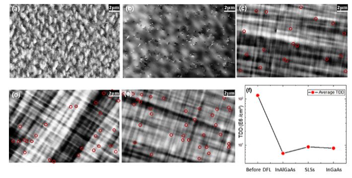
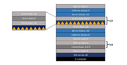
The growth of low-threading-dislocation-density GaAs buffer layers on Si substrates
Monolithic integration of III–V optoelectronic devices on Si platform is gaining momentum, since it enables advantages of low cost, less complexity and high yield for mass production. With the aim of achieving advances in monolithic integration, the challenges associated with lattice mismatch between III–V layers and Si substrates must be overcome, as a low density of threading dislocations (TDs) is a prerequisite for the robustness of the integrated devices. In this paper, we have investigated and compare different types of dislocation filter layers (DFLs) from InGaAs asymmetric step-graded buffer layer (ASG), InGaAs/GaAs strained-layer superlattices, and quaternary alloy InAlGaAs ASG, on the functionality of reducing TD density (TDD) for GaAs buffer layers on Si. Compared to other DFLs, the sample with InAlGaAs ASG buffer layer shows the lowest average TDD value and roughness, while the decrease of TDD in the sample with InAlGaAs ASG buffer layer can be understood in terms of the hardening agent role of aluminium in the InAlGaAs ASG. By further optimising the InAlGaAs ASG through thermal cyclic annealing, we successfully demonstrate a low surface TDD of 6.3 ± 0.1 × 106 cm?2 for a 2 ?m GaAs/InAlGaAs ASG buffer layer grown on Si. These results could provide a thin buffer design for monolithic integration of various III–V devices on Si substrates.
Read the full article here: The growth of low-threading-dislocation-density GaAs buffer layers on Si substrates
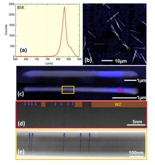
Different Doping Behaviors of Silicon in Zinc Blende and Wurtzite GaAs Nanowires: Implications for Crystal-Phase Device Design
Crystal-phase engineering between zinc blende (ZB) and wurtzite (WZ) structures is becoming an important method in designing unique optoelectronic and electronic semiconductor devices. Doping to engineer their electric properties is thus of critical importance, but a direct experimental comparison in doping these two crystal structures is still missing. Nanowires (NWs) allow the coexistence of both structures due to their special growth mode. The differences in dopant incorporation between the two phases are studied here in GaAs NW shells that are coherently grown around the NWs, hence maintaining the crystal structure of the core. The Si dopant is observed to have a higher incorporation efficiency into the WZ structure due to a 2 times lower incorporation energy compared with that of the ZB structure. Besides, it can also be predicted that Si is more inclined toward Ga sites in both structures. Indeed, the As-site doping energy of the WZ structure is several orders of magnitude higher than that of Ga sites, allowing a lower doping compensation effect. This work provides useful information for doping control and hence designing crystal-phase devices.
Read the full article: Different Doping Behaviors of Silicon in Zinc Blende and Wurtzite GaAs Nanowires: Implications for Crystal-Phase Device Design
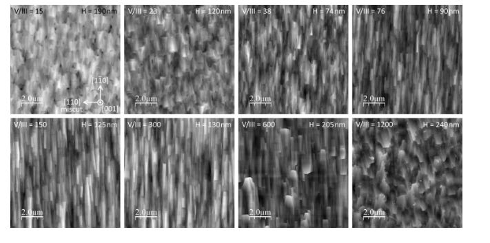
MOVPE studies of zincblende GaN on 3C-SiC/Si(001)
Cubic zincblende GaN films were grown by metalorganic vapour-phase epitaxy on 3C-SiC/Si (001) templates and characterized using Nomarski optical microscopy, atomic force microscopy, X-ray diffraction, and transmission-electron microscopy. In particular, structural properties were investigated of films where the growth temperature of a GaN epilayer varied in the range of 830 degrees C to 910 degrees C and the gas-phase V/III-ratio varied from 15 to 1200 at a constant reactor pressure of 300 Torr. It was observed that with increasing epi temperature at a constant V/III-ratio of 76, the film surface consisted of micrometer-sized elongated features aligned along [1-10] up to a temperature of 880 degrees C. The zincblende phase purity of such samples was generally high with a wurtzite fraction of less than 1%. When grown above 880 degrees C the GaN surface morphology degraded and the zincblende phase purity reduced as a result of inclusions with the wurtzite phase. A progressive narrowing of the 002 reflection with increasing epi growth temperature suggested an improvement of the film mosaicity. With increasing V/III-ratio at a constant growth temperature of 880 degrees C, the film surface formed elongated features aligned along [1-10] at V/III values between 38 and 300 but the morphology became granular at both lower and higher V/III values. The zincblende phase purity is high at V/III values below 300. A slight broadening of the 002 X-ray diffraction reflection with increasing V/III-ratio indicated a small degradation of mosaicity. Scanning electron diffraction analyses of cross-sectional transmission-electron micrographs taken of a selection of samples illustrated the spatial distribution, quantity and structure of wurtzite inclusions within the zincblende GaN matrix. Within the limits of this study, the optimum epilayer growth conditions at a constant pressure of 300 Torr were identified to be at a temperature around 860 degrees C to 880 degrees C and a V/III-ratio in the range of 23 to 76, resulting in relatively smooth, zincblende GaN films without significant wurtzite contamination.
Read the full article: MOVPE studies of zincblende GaN on 3C-SiC/Si(001)
High Operating Temperature Mid-Infrared InGaAs/GaAs Submonolayer Quantum Dot Quantum Cascade Detectors on Silicon
Monolithic integration of infrared photodetectors on a silicon platform is a promising solution for the development of scalable and affordable photodetectors and infrared focal plane arrays. We report on integration of submonolayer quantum dot quantum cascade detectors (SML QD QCDs) on Si substrates via direct growth. Threading dislocation density has been reduced to the level of similar to 10(7) cm(-2) with the high-quality GaAs-on-Si virtual substrate. We also conducted a morphology analysis for the SML QD QCDs through a transmission electron microscope strain contrast image and to the best of our knowledge, high quality InGaAs/GaAs SML QDs were clearly observed on silicon for the first time. Photoluminescence decay time of the as-grown SML QD QCDs on Si was measured to be around 300 ps, which is comparable to the reference QCDs on lattice-matched GaAs substrates. With the high-quality III-V epitaxial layers and SML QDs, the quantum cascade detectors on Si achieved a normal incident photoresponse temperature up to 160 K under zero bias.
Read the full article: High Operating Temperature Mid-Infrared InGaAs/GaAs Submonolayer Quantum Dot Quantum Cascade Detectors on Silicon
Monolithically integrated photonic crystal surface emitters on silicon with a vortex beam by using bound states in the continuum
Optical resonant cavities with high quality factor (Q-factor) are widely used in science and technology for their capabilities of strong confinement of light and enhanced light–matter interaction. The 2D photonic crystal structure with bound states in the continuum (BICs) is a novel concept for resonators with ultra-compact device size, which can be used to generate surface emitting vortex beams based on symmetry-protected BICs at the ? point. Here, to the best of our knowledge, we demonstrate the first photonic crystal surface emitter with a vortex beam by using BICs monolithically grown on CMOS-compatible silicon substrate. The fabricated quantum-dot BICs-based surface emitter operates at 1.3 µm under room temperature (RT) with a low continuous wave (CW) optically pumped condition. We also reveal the BIC’s amplified spontaneous emission with the property of a polarization vortex beam, which is promising to provide a novel degree of freedom in classical and quantum realms.
Read the full article: Monolithically integrated photonic crystal surface emitters on silicon with a vortex beam by using bound states in the continuum
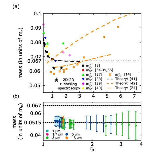
Decoupling of the many-body effects from the electron mass in GaAs by means of reduced dimensionality.
Determining the (bare) electron mass m0 in crystals is often hindered by many-body effects since Fermi -liquid physics renormalizes the band mass, making the observed effective mass m* depend on density. Here, we use a one-dimensional (1D) geometry to amplify the effect of interactions, forcing the electrons to form a nonlinear Luttinger liquid with separate holon and spinon bands, therefore separating the interaction effects from m0. Measuring the spectral function of gated quantum wires formed in GaAs by means of magnetotunnelling spectroscopy and interpreting them using the 1D Fermi-Hubbard model, we obtain m0 = (0.0525 +/- 0.0015)me in this material, where me is the free-electron mass. By varying the density in the wires, we change the interaction parameter rs in the range from similar to 1-4 and show that m0 remains constant. The determined value of m0 is similar to 22% lighter than observed in GaAs in geometries of higher dimensionality D (D > 1), consistent with the quasiparticle picture of a Fermi liquid that makes electrons heavier in the presence of interactions.
Read the full article: Decoupling of the many-body effects from the electron mass in GaAs by means of reduced dimensionality
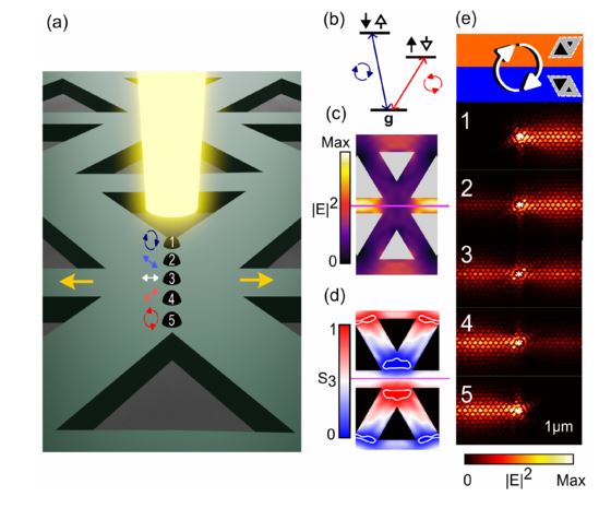
Observation of large spontaneous emission rate enhancement of quantum dots in a broken-symmetry slow-light waveguide.
Quantum states of light and matter can be manipulated on the nanoscale to provide a technological resource for aiding the implementation of scalable photonic quantum technologies. Experimental progress relies on the quality and efficiency of the coupling between photons and internal spin states of quantum emitters. Here we demonstrate a nanophotonic waveguide platform with embedded quantum dots (QDs) that enables both Purcell-enhanced emission and strong chiral coupling. The design uses slow-light effects in a glide-plane photonic crystal waveguide with QD tuning to match the emission frequency to the slow-light region. Simulations were used to map the chirality and Purcell enhancement depending on the position of a dipole emitter relative to the air holes. The highest Purcell factors and chirality occur in separate regions, but there is still a significant area where high values of both can be obtained. Based on this, we first demonstrate a record large radiative decay rate of 17 +/- 2 ns(-1) (60 +/- 6 ps lifetime) corresponding to a 20 +/- 2 fold Purcell enhancement. This was achieved by electric-field tuning of the QD to the slow-light region and quasi-resonant phonon-side band excitation. We then demonstrate a 5 +/- 1 fold Purcell enhancement for a dot with high degree of chiral coupling to waveguide modes, substantially surpassing all previous measurements. Together these demonstrate the excellent prospects for using QDs in scalable implementations of on-chip spin-photonics relying on chiral quantum optics.
Read the full article: Observation of large spontaneous emission rate enhancement of quantum dots in a broken-symmetry slow-light waveguide
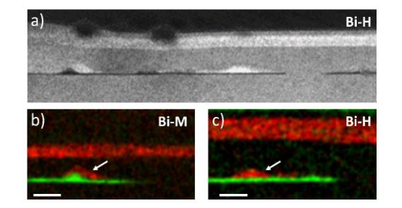
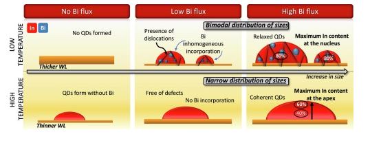
Exploring the formation of InAs(Bi)/GaAs QDs at two growth-temperature regimes under different Bi supply conditions.
The effect of a Bi supply on the development of InAs/GaAs (001) QDs has been structurally explored in two growth temperature regimes, one for Bi alloying (380 degrees C) and another for conventional formation of InAs QDs (510 degrees C). At high growth temperature (HT), there is no trace of Bi incorporation into the film and Bi acts as a surfactant limiting the diffusion length of In. All HT QDs are coherent and free of defects with an inverted coneshaped In distribution. Increasing the Bi supply increases both the QD size and the In content (up to 40 %), while decreasing their areal density. At low temperature (LT), the addition of Bi goes beyond the surfactant role, promoting the transformation of the growth mode from 2D to 3D, resulting in an exponential increase in the QD size with Bi supply. Based on size, these LT QDs are divided into two populations in which the larger QDs relax plastically through the formation of misfit dislocations. LT QDs grown under a Bi flux reach a higher In content (80 %) with a homogeneous distribution within them. Remarkably, incorporation of Bi into larger QDs has been detected but it is not homogeneously distributed.
Read the full article: Exploring the formation of InAs(Bi)/GaAs QDs at two growth-temperature regimes under different Bi supply conditions
The epitaxial growth and unique morphology of InAs quantum dots embedded in a Ge matrix
In this work, we investigate the epitaxial growth of InAs quantum dots (QDs) on Ge substrates. By varying the growth parameters of growth temperature, deposition thickness and the growth rate of InAs, high density (1.2 x 10(11) cm(-2)) self-assembled InAs QDs were successfully epitaxially grown on Ge substrates by solid-source molecular beam epitaxy and capped by Ge layers. Pyramid- and polyhedral-shaped InAs QDs embedded in Ge matrices were revealed, which are distinct from the lens- or truncated pyramid-shaped dots in InAs/GaAs or InAs/Si systems. Moreover, with a 200 nm Ge capping layer, one-third of the embedded QDs are found with elliptical and hexagonal nanovoids with sizes of 7-9 nm, which, to the best of our knowledge, is observed for the first time for InAs QDs embedded in a Ge matrix. These results provide a new possibility of integrating InAs QD devices on group-IV platforms for Si photonics.
Read full article: The epitaxial growth and unique morphology of InAs quantum dots embedded in a Ge matrix

Monolithically Integrated Ultralow Threshold Topological Corner State Nanolasers on Silicon
Monolithic integration of energy-efficient and ultracompact light sources on an industry-standard Si platform has emerged as a promising technology to realize fully integrated Si-based photonic integrated circuits. Recently, semiconductor topological lasers using topologically protected defect modes have received extensive investigation, owing to their unique merits, including robustness against structural imperfections and disorders. However, due to the significant material dissimilarities between Si and III-V materials, previous demonstrations of semiconductor topological lasers have been limited to their native substrates. Here, we experimentally report ultralow threshold, continuous wave, optically pumped, single-mode, InAs/GaAs quantum dot, topological corner state nanolasers monolithically integrated on a CMOS-compatible Si (001) substrate. Our results represent a new route toward ultracompact and high performance integrated nanoscale light sources for Si photonics and enable promising applications for topological photonics.
Read the full article: Monolithically Integrated Ultralow Threshold Topological Corner State Nanolasers on Silicon
Droplet epitaxy of InAs/InP quantum dots via MOVPE by using an InGaAs interlayer
InAs quantum dots (QDs) are grown on an In0.53Ga0.47As interlayer and embedded in an InP(100) matrix. They are fabricated via droplet epitaxy (DE) in a metal organic vapor phase epitaxy (MOVPE) reactor. Formation of metallic indium droplets on the In0.53Ga0.47As lattice-matched layer and their crystallization into QDs is demonstrated for the first time in MOVPE. The presence of the In0.53Ga0.47As layer prevents the formation of an unintentional non-stoichiometric 2D layer underneath and around the QDs, via suppression of the As-P exchange. The In0.53Ga0.47As layer affects the surface diffusion leading to a modified droplet crystallization process, where unexpectedly the size of the resulting QDs is found to be inversely proportional to the indium supply. Bright single dot emission is detected via micro-photoluminescence at low temperature, ranging from 1440 to 1600 nm, covering the technologically relevant telecom C-band. Transmission electron microscopy investigations reveal buried quantum dots with truncated pyramid shape without defects or dislocations.
Read full paper: Droplet epitaxy of InAs/InP quantum dots via MOVPE by using an InGaAs interlayer
A thermally erasable silicon oxide layer for molecular beam epitaxy
We present a systematic study of the oxidation and deoxidation behaviours of several kinds of ultrathin silicon oxide layers frequently used in silicon (Si) technology, which in this work serve as surface protecting layers for molecular beam epitaxy (MBE). With various characterization techniques, we demonstrate that a chemically grown silicon oxide layer is the most promising candidate for subsequent removal in an ultra-high vacuum chamber at a temperature of 1000 C-circle, without making use of a reducing agent. As a demonstration, a tensile-strained Ge(100) layer is epitaxially grown on the deoxidised wafer with an atomically flat surface and a low threading dislocation density of 3.33 x 10(8) cm(-2). Our findings reveal that the ultra-thin oxide layer grown using a chemical approach is able to protect Si surfaces for subsequent MBE growth of Ge. This approach is promising for the growth of III/V-on-Si (using Ge as a buffer) and all group-IV related epitaxy for integration on the Si photonics platforms.
Read the full article: A thermally erasable silicon oxide layer for molecular beam epitaxy
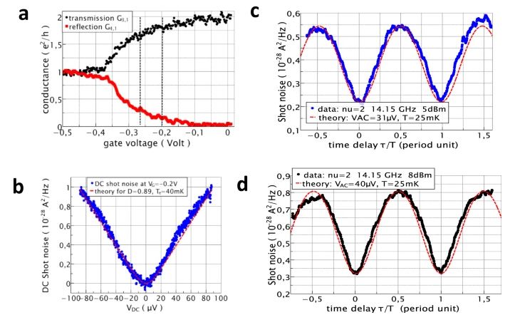
Two-particle time-domain interferometry in the fractional quantum Hall effect regime
Quasi-particles are elementary excitations of condensed matter quantum phases. Demonstrating that they keep quantum coherence while propagating is a fundamental issue for their manipulation for quantum information tasks. Here, we consider anyons, the fractionally charged quasi-particles of the Fractional Quantum Hall Effect occurring in two-dimensional electronic conductors in high magnetic fields. They obey anyonic statistics, intermediate between fermionic and bosonic. Surprisingly, anyons show large quantum coherence when transmitted through the localized states of electronic Fabry-Pérot interferometers, but almost no quantum interference when transmitted via the propagating states of Mach-Zehnder interferometers. Here, using a novel interferometric approach, we demonstrate that anyons do keep quantum coherence while propagating. Performing two-particle time-domain interference measurements sensitive to the two-particle Hanbury Brown Twiss phase, we find 53 and 60% visibilities for anyons with charges e/5 and e/3. Our results give a positive message for the challenge of performing controlled quantum coherent braiding of anyons.
Read full article: https://www-nature-com.sheffield.idm.oclc.org/articles/s41467-022-33603-3
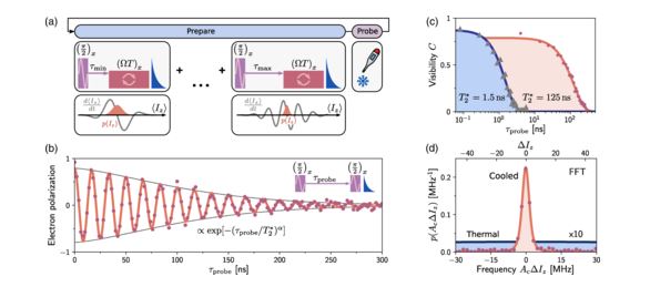
Optimal Purification of a Spin Ensemble by Quantum-Algorithmic Feedback
Purifying a high-temperature ensemble of quantum particles toward a known state is a key requirement to exploit quantum many-body effects. An alternative to passive cooling, which brings a system to its ground state, is active feedback, which stabilizes the system at a chosen target state. This alternative, if realized, offers additional control capabilities for the design of quantum states. Here we present a feedback algorithm applied to a quantum system, which is capable of stabilizing the collective state of an ensemble from its maximum entropy state to the limit of single quantum fluctuations. Our algorithmic approach maximizes the rate of state purification given the system’s physical constants; thus it remains the optimal feedback approach even in the presence of dissipation and disorder. We test experimentally the robustness of this feedback on the highly inhomogeneous nuclear-spin ensemble of a semiconductor quantum dot, reducing nuclear-spin fluctuations 83-fold, down to 5.7(2) spin macrostates. Simulations demonstrate that without system-specific inhomogeneities, our algorithm can purify the system down to single-spin fluctuations. Further, we exploit our algorithmic approach to tailor nontrivial nuclear-spin distributions that go beyond simple polarization, including weighted bimodality and latticed multistability. This control is a precursor toward quantum-correlated macrostates, which an extended version of our algorithm could generate in homogeneous systems.
Read full article: https://journals-aps-org.sheffield.idm.oclc.org/prx/abstract/10.1103/PhysRevX.12.031014
Single-Mode Photonic Crystal Nanobeam Lasers Monolithically Grown on Si for Dense Integration
Ultra-compact III-V nanolasers monolithically integrated on Si with ultra-low energy consumption and small modal volume have been emerged as one of the most promising candidates to achieve Si on-chip light sources. However, the significant material dissimilarities between III-V and Si fundamentally limit the performance of Si-based III-V nanolasers. In this work, we report 1.3 mu m InAs/GaAs quantum-dot photonic-crystal (PhC) nanobeam lasers directly grown on complementary metal-oxide-semiconductor compatible on-axis Si (001) substrates. The continuous-wave optically pumped PhC nanobeam lasers exhibited a single-mode operation, with an ultra-low lasing threshold of similar to 0.8 mu W at room temperature. In addition, a nanoscale physical volume of similar to 8 x 0.53 x 0.36 mu m(3) (similar to 25 (lambda n(-1))(3)) was realized through a small number of air-holes in PhC nanobeam laser. The promising characteristics of the PhC nanobeam lasers with small footprint and ultra-low energy consumption show their advanced potential towards densely integrated Si photonic integrated circuits.
Read the full article: Single-Mode Photonic Crystal Nanobeam Lasers Monolithically Grown on Si for Dense Integration
Control of Morphology and Substrate Etching in InAs/InP Droplet Epitaxy Quantum Dots for Single and Entangled Photon Emitters
We present a detailed atomic-resolution study of morphology and substrate etching mechanism in InAs/InP droplet epitaxy quantum dots (QDs) grown by metal–organic vapor phase epitaxy via cross-sectional scanning tunneling microscopy (X-STM). Two different etching processes are observed depending on the crystallization temperature: local drilling and long-range etching. In local drilling occurring at temperatures of ?500 °C, the In droplet locally liquefies the InP underneath and the P atoms can easily diffuse out of the droplet to the edges. During crystallization, the As atoms diffuse into the droplet and crystallize at the solid–liquid interface, forming an InAs etch pit underneath the QD. In long-range etching, occurring at higher temperatures of >500 °C, the InP layer is destabilized and the In atoms from the surroundings migrate toward the droplet. The P atoms can easily escape from the surface into the vacuum, forming trenches around the QD. We show for the first time the formation of trenches and long-range etching in InAs/InP QDs with atomic resolution. Both etching processes can be suppressed by growing a thin layer of InGaAs prior to the droplet deposition. The QD composition is estimated by finite element modeling in combination with X-STM. The change in the morphology of QDs due to etching can strongly influence the fine structure splitting. Therefore, the current atomic-resolution study sheds light on the morphology and etching behavior as a function of crystallization temperature and provides a valuable insight into the formation of InAs/InP droplet epitaxy QDs which have potential applications in quantum information technologies.
Read full article: Control of Morphology and Substrate Etching in InAs/InP Droplet Epitaxy Quantum Dots for Single and Entangled Photon Emitters
Influence of Al (x) Ga1-x N nucleation layers on MOVPE-grown zincblende GaN epilayers on 3C-SiC/Si(001)
The suitability of AlxGa1-xN nucleation layers (NLs) with varying Al fraction x for the metal organic vapour phase epitaxy of zincblende GaN on (001) 3C-SiC was investigated, using x-ray photoelectron spectroscopy, atomic force microscopy, and x-ray diffraction. The as-grown NLs exhibited elongated island structures on their surface, which reduce laterally into smaller, more equiaxed islands with increasing AlN composition. During high-temperature annealing in a mixture of NH3 and H2 the nucleation islands with low Al fraction ripened and increased in size, whereas this effect was less pronounced in samples with higher Al fraction. The compressive biaxial in-plane strain of the NLs increases with increasing AlN composition up to x = 0.29. GaN epilayers grown over NLs that have low Al fraction have high cubic zincblende phase purity and are slightly compressively strained relative to 3C-SiC. However, those samples with a measured Al fraction in the NL higher than 0.29 were predominantly of the hexagonal wurtzite phase, due to formation of wurtzite inclusions on various {111} facets of zb-GaN, thus indicating the optimal Al composition for phase-pure zb-GaN epilayer growth.
Read full article: https://iopscience-iop-org.sheffield.idm.oclc.org/article/10.1088/1361-6463/ac4c58
Recent Progress of Quantum Dot Lasers Monolithically Integrated on Si Platform
With continuously growing global data traffic, silicon (Si)-based photonic integrated circuits have emerged as a promising solution for high-performance Intra-/Inter-chip optical communication. However, a lack of a Si-based light source remains to be solved due to the inefficient light-emitting property of Si. To tackle the absence of a native light source, integrating III-V lasers, which provide superior optical and electrical properties, has been extensively investigated. Remarkably, the use of quantum dots as an active medium in III-V lasers has attracted considerable interest because of various advantages, such as tolerance to crystalline defects, temperature insensitivity, low threshold current density and reduced reflection sensitivity. This paper reviews the recent progress of III-V quantum dot lasers monolithically integrated on the Si platform in terms of the different cavity types and sizes and discusses the future scope and application.
Read full article: Recent Progress of Quantum Dot Lasers Monolithically Integrated on Si Platform

Nanoscale wafer patterning using SPM induced local anodic oxidation in InP substrates
Atomic force microscopy (AFM) assisted local anodic oxidation (LAO) offers advantages over other semiconductor fabrication techniques as it is a low contamination method. We demonstrate the fabrication of deep and highly reproducible nanohole arrays on InP using LAO. Nanohole and nano-oxide mound radius and depth are controlled independently by altering AFM tip bias and humidity, with a maximum nanohole depth of 15.6 ± 1.2 nm being achieved. Additionally, the effect of tip write speed on oxide line formation is compared for n-type, p-type and semi-insulating substrates, which shows that n-type InP oxidizes at a slower rate that semi-insulated or p-type InP. Finally, we calculate the activation energy for LAO of semi-insulating InP to be 0.4 eV, suggesting the oxidation mechanism is similar to that which occurs during plasma oxidation.
Read full article: https://iopscience-iop-org.sheffield.idm.oclc.org/article/10.1088/1361-6641/ac3f20

Directly correlated microscopy of trench defects in InGaN quantum wells
Directly correlated measurements of the surface morphology, light emission and subsurface structure and composition were carried out on the exact same nanoscale trench defects in InGaN quantum well (QW) structures. Multiple scanning probe, scanning electron and transmission electron microscopy techniques were used to explain the origin of their unusual emission behaviour and the relationship between surface morphology and cathodoluminescence (CL) redshift. Trench defects comprise of an open trench partially or fully enclosing material in InGaN QWs with different CL emission properties to their surroundings. The CL redshift was shown to typically vary with the width of the trench and the prominence of the material enclosed by the trench above its surroundings. Three defects, encompassing typical and atypical features, were prepared into lamellae for transmission electron microscopy (TEM). A cross marker technique was used in the focused ion beam-scanning electron microscope (FIB-SEM) to centre the previously characterised defects in each lamella for further analysis. The defects with wider trenches and strong redshifts in CL emission had their initiating basal-plane stacking fault (BSF) towards the bottom of the QW stack, while the BSF formed near the top of the QW stack for a defect with a narrow trench and minimal redshift. The raised-centre, prominent defect showed a slight increase in QW thickness moving up the QW stack while QW widths in the level-centred defect remained broadly constant. The indium content of the enclosed QWs increased above the BSF positions up to a maximum, with an increase of approximately 4% relative to the surroundings seen for one defect examined. Gross fluctuations in QW width (GWWFs) were present in the surrounding material in this sample but were not seen in QWs enclosed by the defect volumes. These GWWFs have been linked with indium loss from surface step edges two or more monolayers high, and many surface step edges appear pinned by the open trenches, suggesting another reason for the higher indium content seen in QWs enclosed by trench defects.
Read full article: https://www-sciencedirect-com.sheffield.idm.oclc.org/science/article/pii/S0304399121000474?via%3Dihub
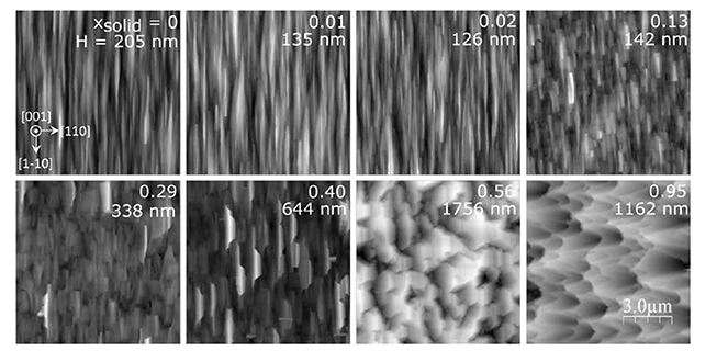
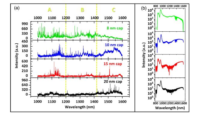
Effect of Cap Thickness on InAs/InP Quantum Dots Grown by Droplet Epitaxy in Metal–Organic Vapor Phase Epitaxy
InAs quantum dots (QDs) are grown on bare InP(001) via droplet epitaxy (DE) in metal–organic vapor phase epitaxy (MOVPE). Capping layer engineering, used to control QD size and shape, is explored for DE QDs in MOVPE. The method allows for the tuning of the QD emission over a broad range of wavelengths, ranging from the O- to the L-band. The effect of varying the InP capping layer is investigated optically by macro- and micro-photoluminescence (PL, µPL) and morphologically by transmission electron microscopy (TEM). A strong 500?nm blueshift of the QD emission wavelength is observed when the capping layer is reduced from 20 to 8?nm, which is reflected by a clear size reduction of the buried QDs.
Read full article: Effect of Cap Thickness on InAs/InP Quantum DotsGrown by Droplet Epitaxy in Metal–Organic Vapor Phase Epitaxy
All-MBE grown InAs/GaAs quantum dot lasers with thin Ge buffer layer on Si substrates
A high-performance III-V quantum-dot (QD) laser monolithically grown on Si is one of the most promising candidates for commercially viable Si-based lasers. Great efforts have been made to overcome the challenges due to the heteroepitaxial growth, including threading dislocations and anti-phase boundaries, by growing a more than 2 mu m thick III-V buffer layer. However, this relatively thick III-V buffer layer causes the formation of thermal cracks in III-V epi-layers, and hence a low yield of Si-based optoelectronic devices. In this paper, we demonstrate a usage of thin Ge buffer layer to replace the initial part of GaAs buffer layer on Si to reduce the overall thickness of the structure, while maintaining a low density of defects in III-V layers and hence the performance of the InAs/GaAs QD laser. A very high operating temperature of 130 degrees C has been demonstrated for an InAs/GaAs QD laser by this approach.
Read full article: All-MBE grown InAs/GaAs quantum dot lasers with thin Ge buffer layer on Si substrates
Heteroepitaxial Growth of III-V Semiconductors on Silicon
Monolithic integration of III-V semiconductor devices on Silicon (Si) has long been of great interest in photonic integrated circuits (PICs), as well as traditional integrated circuits (ICs), since it provides enormous potential benefits, including versatile functionality, low-cost, large-area production, and dense integration. However, the material dissimilarity between III-V and Si, such as lattice constant, coefficient of thermal expansion, and polarity, introduces a high density of various defects during the growth of III-V on Si. In order to tackle these issues, a variety of growth techniques have been developed so far, leading to the demonstration of high-quality III-V materials and optoelectronic devices monolithically grown on various Si-based platform. In this paper, the recent advances in the heteroepitaxial growth of III-V on Si substrates, particularly GaAs and InP, are discussed. After introducing the fundamental and technical challenges for III-V-on-Si heteroepitaxy, we discuss recent approaches for resolving growth issues and future direction towards monolithic integration of III-V on Si platform.
Read the full article: Heteroepitaxial Growth of III-V Semiconductors on Silicon
Optical analogue of Dresselhaus spin-orbit interaction in photonic graphene
The concept of gauge fields plays a significant role in many areas of physics, from particle physics and cosmology to condensed-matter systems, where gauge potentials are a natural consequence of electromagnetic fields acting on charged particles and are of central importance in topological states of matter(1). Here, we report on the experimental realization of a synthetic non-Abelian gauge field for photons(2) in a honeycomb microcavity lattice(3). We show that the effective magnetic field associated with transverse electric-transverse magnetic splitting has the symmetry of the Dresselhaus spin-orbit interaction around Dirac points in the dispersion, and can be regarded as an SU(2) gauge field(4). The symmetry of the field is revealed in the optical spin Hall effect, where, under resonant excitation of the Dirac points, precession of the photon pseudospin around the field direction leads to the formation of two spin domains. Furthermore, we observe that the Dresselhaus-type field changes its sign in the same Dirac valley on switching from s to p bands, in good agreement with the tight-binding modelling. Our work demonstrating a non-Abelian gauge field for light on the microscale paves the way towards manipulation of photons via spin on a chip.
A spin-orbit coupling effect in photonic graphene made of coupled polaritonic microcavities is experimentally realized, revealing the unique fine structure of the eigenstates around the Dirac points, with the formation of a Dresselhaus-like effective magnetic field that can be mapped to a non-Abelian gauge field.
Read full paper: Optical analogue of Dresselhaus spin-orbit interaction in photonic graphene
Purcell enhancement of a deterministically coupled quantum dot in an SU-8 laserpatterned photonic crystal heterostructure.
Enhancement of single photon source emission through cavity quantum electrodynamics is key to the realization of applicable emitters in
many quantum optics technologies. In this work, we present a flexible and convenient cavity fabrication process that writes a SU-8 microstrip onto a photonic crystal waveguide deterministically, in which InGaAs/GaAs quantum dots are present as emitters. The strip cavity is laser patterned at the location of a quantum dot with a chosen emission wavelength. Micro- photoluminescence studies are undertaken, which demonstrate an enhanced emission intensity by a factor of 2.1 with weak coupling to a single quantum dot, and time-resolved photoluminescence further shows a Purcell enhancement factor of 2.16. The fabrication process is, thus, verified as a reliable recipe to introduce deterministic cavity coupling to a chosen quantum dot.
Read full article: Purcell enhancement of a deterministically coupled quantum dot …5.0018673
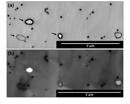
InAs/InP Quantum Dots in Etched Pits by Droplet Epitaxy in Metalorganic Vapor Phase Epitaxy
The growth of InAs quantum dots (QDs) on InP(100) via droplet epitaxy in a metalorganic vapor phase epitaxy (MOVPE) reactor is studied. Formation of indium droplets is investigated with varying substrate temperature, and spontaneous formation of nanoholes is observed for the first time under MOVPE conditions. Indium droplets are crystallized into QDs under arsenic flow at
different temperatures. For temperatures greater than 500 C, a local etching takes place in the QD vicinity, showing an unexpected morphology which is found to be strongly dependent on the crystallization conditions. Such QDs are structurally and optically investigated and emission from single QDs in the telecom C-band is detected via microphotoluminescence at low temperature.
Read full article: InAs-InP Quantum Dots … Sala et al pssr.202000173
Continuous-wave quantum dot photonic crystal lasers grown on on-axis Si (001).
Semiconductor III–V photonic crystal (PC) laser is regarded as a promising ultra-compactlight source with unique advantages of ultralow energy consumption and small footprint for the next generation of Si-based on-chip optical interconnects. However, the significant material dissimilarities between III-V materials and Si are the fundamental roadblock for conventional monolithic III-V-on-silicon integration technology. Here, we demonstrate ultrasmall III-V PC membrane lasers monolithically grown on CMOS-compatible on-axis Si(001) substrates by using III-V quantum dots. The optically pumped InAs/GaAs quantum-dot PC lasers exhibit single-mode operation with an ultra-low threshold of ~0.6uW and a large spontaneous emission coupling efficiency up to 18% under continuous-wave condition at room temperature. This work establishes a new route to form the basis of future mono-lithic light sources for high-density optical interconnects in future large-scale silicon elec-tronic and photonic integrated circuits.
Read full article: Continuous-wave quantum dot photonic crystal lasers grown on on-axis Si (001). s41467-020-14736-9
A semiconductor topological photonic ring resonator
Unidirectional photonic edge states arise at the interface between two topologically distinct photonic crystals. Here, we demonstrate a micrometer-scale GaAs photonic ring resonator, created using a spin Hall-type topological photonic crystal waveguide. Embedded InGaAs
quantum dots are used to probe the mode structure of the device. We map the spatial profile of the resonator modes and demonstrate the control of the mode confinement through tuning of the photonic crystal lattice parameters. The intrinsic chirality of the edge states makes them of interest for applications in integrated quantum photonics, and the resonator represents an important building block toward the development of such devices with embedded quantum emitters.
Read full article: A semiconductor topological photonic ring
Quantum teleportation using highly coherent emission from telecom C-band quantum dots
A practical way to link separate nodes in quantum networks is to send photons over the standard telecom fibre network. This requires sub-Poissonian photon sources in the wavelength band around 1550 nm, with photon coherence times sufficient to enable
the many interference-based technologies at the heart of quantum networks. Here, we show that droplet epitaxy InAs/InP quantum dots emitting in the telecom C-band can provide photons with coherence times exceeding 1 ns under low power non-resonant excitation, and demonstrate that these coherence times enable near-optimal interference with a C-band polarisation-encoded laser qubit, with visibilities only limited by the quantum dot multiphoton emission. Using entangled photons, we further show teleportation of such qubits in six different bases with average postselected fidelity reaching 88.3 ± 4.0%. Beyond direct
applications in long-distance quantum communication, the high degree of coherence in these quantum dots is promising for future spin-based telecom quantum network applications.
Read full article: Quantum teleportation using highly coherent emission …npjQI6_14-1
Optical spin locking of a solid-state qubit
Quantum control of solid-state spin qubits typically involves pulses in the microwave domain, drawing from the well-developed toolbox of magnetic resonance spectroscopy. Driving a solid-state spin by optical means offers a high-speed alternative, which in the presence of limited spin coherence makes it the preferred approach for high-fidelity quantum control. Bringing the full versatility of magnetic spin resonance to the optical domain requires full phase and amplitude control of the optical fields. Here, we imprint a programmable microwave sequence onto a laser field and perform electron spin resonance in a semiconductor quantum dot via a two-photon Raman process. We show that this approach yields full SU(2) spin control with over 98%?-rotation fidelity. We then demonstrate its versatility by implementing a particular multi-axis control sequence, known as spin locking. Combined with electron-nuclear Hartmann–Hahn resonances which we also report in this work, this sequence will enable efficient coherent transfer of a quantum state from the electron spin to the mesoscopic nuclear ensemble.
Read full article: Optical spin locking of a solid-state qubit npjQI5_95-1
Thick, adherent diamond films on AlN with low termal barrier resistance
The growth of >100-?m-thick diamond layersadherent on aluminum nitride with low thermal boundaryresistance between diamond and AlN is presented in this work. The thermal barrier resistance was found to be in therange of 16 m2·K/GW, which is a large improvement on thecurrent state-of-the-art. While thickfilms failed to adhere onuntreated AlNfilms, AlNfilms treated with hydrogen/nitrogen plasma retained the thick diamond layers. Cleardifferences in?-potential measurement confirm surfacemodification due to hydrogen/nitrogen plasma treatment. An increase in non-diamond carbon in the initial layers ofdiamond grown on pretreated AlN is seen by Ramanspectroscopy. The presence of non-diamond carbon has minimal effect on the thermal barrier resistance. The surfaces studiedwith X-ray photoelectron spectroscopy revealed a clear distinction between pretreated and untreated samples. The surfacealuminum goes from a nitrogen-rich environment to an oxygen-rich environment after pretreatment. A clean interface betweendiamond and AlN is seen by cross-sectional transmission electron microscopy.
Read full article: Thick, adherent diamond films on AlN with low thermal barrier resistance
Telecommunication wavelength confined Tamm plasmon structures containing InAs/GaAs quantum dot emitters at room temperature
We experimentally demonstrate gold microdisc structures that produce confined Tamm plasmons (CTPs) – interface modes between a metal layer and a distributed Bragg reflector – resonant around 1.3 um. Quantum dots grown within the structures show an order of magnitude increase in the photoluminescence emitted at room temperature. Varying the disc diameter, we show spectral tuning of the resonance and measure the dispersion relation as evidence of mode confinement. The simplicity of fabrication and tuneability of these structures make CTPs an ideal platform for making scalable telecom devices based on quantum dots.
Read full article: Telecommunication wavelength confined Tamm plasmon structures containing InAs/GaAs quantum dot emitters at room temperature
Confined Tamm optical states coupled to quantum dots in a photoconductive detector
By employing Tamm optical states—states localized between a thin metal microdisk and a semiconductor distributed Bragg reflector—we demonstrate near 1300nm (O-band), narrow wavelength (20nm FWHM), highly spatially localized photodetection. By varying the size of the microdisk, we show spectral tuning (7 nm) of the peak optical response. Furthermore, by reducing the symmetry of the microstructures, we lift the degeneracy of the polarization, producing a polarization sensitivity in our detector. These confined Tamm states are useful not only for sensing but also for photoconductive switch applications such as optical microwave switches and terahertz generation.
Read full article: Confined Tamm optical states coupled to quantum dots in a photoconductive detector
A comparative study of epitaxial InGaAsBi/InP structures using Rutherford backscattering spectrometry, X-ray diffraction and photoluminescence techniques
In this work, we used a combination of photoluminescence (PL), high resolution X-ray diffraction (XRD), and Rutherford backscattering spectrometry (RBS) techniques to investigate material quality and structural properties of MBE-grown InGaAsBi samples (with and without an InGaAs cap layer) with targeted bismuth composition in the 3%–4% range. XRD data showed that the InGaAsBi layers are more homo-geneous in the uncapped samples. For the capped samples, the growth of the InGaAs capped layer at higher temperature affects the quality of the InGaAsBi layer and bismuth distribution in the growth direction. Low-temperature PL exhibited multiple emission peaks; the peak energies, widths, and relative intensities were used for comparative analysis of the data in line with the XRD and RBS results. RBS data at a random orientation together with channeled measurements allowed both an estimation of the bismuth composition and analysis of the structural properties. The RBS channeling showed evidence of higher strain due to possible antisite defects in the capped samples grown at a higher temperature. It is also suggested that the growth of the capped layer at high temperature causes deterioration of the bismuth-layer quality. The RBS analysis demonstrated evidence of a reduction of homogeneity of uncapped InGaAsBi layers with increasing bismuth concentration. The uncapped higher bismuth concentration sample showed less defined channeling dips suggesting poorer crystal quality and clustering of bismuth on the sample surface.
Read full article: A comparative study of epitaxial InGaAsBi-InP structures using Rutherfor backscattering spectrometry, X-ray diffraction and photoluminescence techniques
Non-destructive characterization of thin layer resonant tunneling diodes
We present an advanced nondestructive characterization scheme for high current density AlAs/InGaAs resonant tunneling diodes pseudomorphically grown on InP substrates. We show how low-temperature photoluminescence spectroscopy (LT-PL) and high-resolution X-ray diffractometry (HR-XRD) are complementary techniques to increase the confidence of the characterized structure. The lattice-matched InGaAs is characterized and found to be of high quality. We discuss the inclusion of an undoped “copy” well (C-well) in terms of enhancements to HRXRD and LT-PL characterization and quantify the improved precision in determining the structure. As a consequence of this enhanced precision in the determination of physical structure, the AlAs barriers and quantum well (QW) system are found to contain nonideal material interfaces. Their roughness is characterized in terms of the full width to half-maximum of the split LT-PL emission peaks, revealing a ±1 atomic sheet variance to the QW width. We show how barrier asymmetry can be detected through fitting of both optical spectra and HR-XRD rocking curves.
Read full article: Non-destructive characterisation of thin layer resonant tunnelling diodes
Light Scattering from Solid-State Quantum Emitters: Beyond the Atomic Picture
Coherent scattering of light by a single quantum emitter is a fundamental process at the heart of many proposed quantum technologies. Unlike atomic systems, solid-state emitters couple to their host lattice by phonons. Using a quantum dot in an optical nanocavity, we resolve these interactions in both time and frequency domains, going beyond the atomic picture to develop a comprehensive model of light scattering from solid-state emitters. We find that even in the presence of a low-Q cavity with high Purcell enhancement, phonon coupling leads to a sideband that is completely insensitive to excitation conditions and to a nonmonotonic relationship between laser detuning and coherent fraction, both of which are major deviations from atomlike behavior.
Read full article: Light scattering from solid-state quantum emitters: Beyond the atomic picture
Characterisation of Thin-Layer Resonant Tunnelling Diodes grown by MOVPE
Resonant tunneling diodes (RTDs) are next-generation candidates for core THz generation technologies, with proven quasi-optical tunable emission capability, with centre frequencies of 0.1 – 1.98 THz at cca. 1mW, when coupled into a suitable monolithically integrated antenna. For this purpose, the strained InGaAs/AlAs/InP material system is approaching technological maturity, with its offering of high electron mobility, suitable conduction band offsets, and very low resistance contacts. However, the epitaxially thin layers used for RTDs, realise devices with current densities in excess of 10 mA mu m(-2) and electric fields approaching that of the breakdown of the material. As a high current density is a traditional indicator of performance for these oscillators, it is now increasingly important to grow crystalline layers with near-atomic perfection. In previous work, we showed how the inclusion of a nominally identical, un-doped electrically neutral copy of the RTD double barrier – quantum well (QW) system, leads to the observance of a type-II QW emission in addition to the type-I emission from the active region QW. This could be used to establish the quasi-bound elastic energy, whose level is directly correlated to the peak voltage of the N-shape I-V characteristic. Here we extend this approach with the addition of high-resolution X-ray diffractometry and low-temperature photoluminescence spectroscopy. Through a step-by-step process of curve fitting, comparing to simulation and results, we can comment on the quality and thickness of the ternary InGaAs alloy interfaces surrounding the AlAs barriers. These findings are confirmed with scanning transmission electron microscopy.
QUANTUM DOTS AND NANOSTRUCTURES: GROWTH, CHARACTERIZATION, AND MODELING XVI Edited by:Huffaker, DL; Eisele, H
Book Series: Proceedings of SPIE
Volume: 10929
Article Number:1092909
Authors: Baba, R., Kojima, O., Jacobs, K. J. P., Harrison, B. A., Stevens, B. J., Mukai, T., Hogg, R.A.
DOI:10.1117/12.2510119
Published:2019
Document Type:Proceedings Paper
High temperature Alinp X-ray spectrometers
Two custom-made Al0.52In0.48P p(+)-i-n(+) mesa photodiodes with different diameters (217 mu m +/- 15 mu m and 409 mu m +/- 28 mu m) and i layer thicknesses of 6 mu m have been electrically characterised over the temperature range 0 degrees C to 100 degrees C. Each photodiode was then investigated as a high-temperature-tolerant photon counting X-ray detector by connecting it to a custom-made low-noise charge-sensitive preamplifier and illuminating it with an Fe-55 radioisotope X-ray source (Mn K alpha = 5.9 keV; Mn K beta = 6.49 keV). At 100 degrees C, the best energy resolutions (full width at half maximum at 5.9 keV) achieved using the 217 mu m +/- 15 mu m diameter photodiode and the 409 mu m +/- 28 mu m diameter photodiode were 1.31 keV +/- 0.04 keV and 1.64 keV +/- 0.08 keV, respectively. Noise analysis of the system is presented. The dielectric dissipation factor of Al0.52In0.48P was estimated as a function of temperature, up to 100 degrees C. The results show the performance of the thickest Al0.52In0.48P X-ray detectors so far reported at high temperature. The work has relevance for the development of novel space science instrumentation for use in hot space environments and extreme terrestrial applications.
Read full article: High-temperature-alinp-x-ray-spectrometers
InGaP electron spectrometer for high temperature environments
In this work, a 200 mu m diameter InGaP (GaInP) p(+)-i-n(+) mesa photodiode was studied across the temperature range 100 degrees C to 20 degrees C for the development of a temperature-tolerant electron spectrometer. The depletion layer thickness of the InGaP device was 5 mu m. The performance of the InGaP detector was analysed under dark conditions and then under the illumination of a 183 MBq Ni-63 radioisotope beta particle source. The InGaP photodiode was connected to a custom-made low-noise charge-sensitive preamplifier to realise a particle counting electron spectrometer. Beta spectra were collected at temperatures up to 100 degrees C with the InGaP device reverse biased at 5V. The spectrum accumulated at 20 degrees C was compared with the spectrum predicted using Monte Carlo simulations; good agreement was found between the predicted and experimental spectra. The work is of importance for the development of electron spectrometers that can be used for planetary and space science missions to environments of high temperature or extreme radiation (e.g. Mercury, Jupiter’s moon Europa, near-Sun comets), as well as terrestrial applications.
Read full article: Ingap-electron-spectrometer-for-high temperature environments
AlInP photodiode x-ray detectors
Four Al0.52In0.48P p(+)-i-n(+) mesa photodiodes with 6 mu m thick i layers and two different diameters (217 mu m +/- 15 mu m and 409 mu m +/- 28 mu m) were studied at room temperature (24 degrees C). Electrical characterisation measurements are reported along with measurements showing the performance of the devices as x-ray detectors. The devices exhibited leakage currents <3 pA (corresponding to leakage current densities <2 nA cm(-2)) at 100 V reverse bias (electric field strength of 167 kV cm(-1)). The photodiodes were coupled to a custom-made low-noise charge-sensitive preamplifier, the noise characteristics of the resultant spectrometers were investigated as functions of shaping times. The best energy resolutions (full width at half maximum of the 5.9 keV photopeak from an Fe-55 radioisotope x-ray source) achieved with the 217 mu m +/- 15 mu m and 409 mu m +/- 28 mu m diameter photodiodes were 0.89 keV and 1.05 keV, respectively. The dielectric dissipation factor of Al0.52In0.48P was estimated to be (2.2 +/- 1.1) x 10(-3) at room temperature.
Read full article: Alinp-photodiode-x-ray-detectors
Tunable Photon Statistics Exploiting the Fano Effect in a Waveguide
A strong optical nonlinearity arises when coherent light is scattered by a semiconductor quantum dotcoupled to a nanophotonic waveguide. We exploit the Fano effect in such a waveguide to control the phaseof the quantum interference underpinning the nonlinearity, experimentally demonstrating a tunablequantum optical filter which converts a coherent input state into either a bunched or an antibunchednonclassical output state. We show theoretically that the generation of nonclassical light is predicated onthe formation of a two-photon bound state due to the interaction of the input coherent state with thequantum dot. Our model demonstrates that the tunable photon statistics arise from the dependence of thesign of two-photon interference (either constructive or destructive) on the detuning of the input relative tothe Fano resonance.
Read full article: Tunable Photon Statistics Exploiting the Fano Effect in a Waveguide PhysRevLett.122.173603
Improved Planar InAs Avalanche Photodiodes With Reduced Dark Current and Increased Responsivity
Indium Arsenide (InAs) infrared photodiodes provide high quantum efficiency in the wavelength range of 1.0-3.0 mu m. Planar diode configuration has been adopted to reduce surface leakage. In this work, new fabrication procedures for planar InAs avalanche photodiodes (APDs) are reported. Beryllium (Be) ions were implanted into InAs at a relatively low energy of 34 keV. Effects of duration of post implant annealing on the electrical characteristics of InAs APDs were investigated. It was found that a combination of post implant annealing at 500 degrees C for 15 min and a shallow surface etch produces planar APDs with good characteristics (room temperature dark current density of 0.52 A/cm(2) at -0.2 V and external quantum efficiency of 51% at 1520 nm at -0.3 V). These represent a 3 times reduction in dark current and 1.4 times increase in responsivity, compared to earlier Be-implanted planar InAs APDs. The APDs’ avalanche gain characteristics remain similar to those from earlier reports, with a gain of 4 at a relatively low operating bias of 5 V. This suggests the potential of integrating InAs APDs with low voltage readout integrated circuits (ROIC) for development of infrared imaging arrays. The data reported in this paper is available from the ORDA digital repository (DOI: 10.15131/shef.data.6955037).
Read full article: Improved planar InAs avalanche photodiodes with reduced dark current and increased responsivity 10.1109_JLT.2019.2905535
Broadband THz absorption spectrometer based on excitonic nonlinear optical effects
A broadly tunable THz source is realized via difference frequency generation, in which an enhancement to X (3) that is obtained via resonant excitation of III–V semiconductor quantum well excitons is utilized. The symmetry of the quantum wells (QWs) is broken by utilizing the built-in electric-field across a p–i–n junction to produce effective X (2) processes, which are derived from the high X (3). This X (2) media exhibits an onset of nonlinear processes at ~4 W cm-2, thereby enabling area (and, hence, power) scaling of the THz emitter. Phase matching is realized laterally through normal incidence excitation. Using two collimated 130 mW continuous wave (CW) semiconductor lasers with ~1-mm beam diameters, we realize monochromatic THz emission that is tunable from 0.75 to 3 THz and demonstrate the possibility that this may span 0.2–6 THz with linewidths of ~20 GHz and efficiencies of ~1 × 10⁻⁵, thereby realizing ~800 nW of THz power. Then, transmission spectroscopy of atmospheric features is demonstrated, thereby opening the way for compact, low-cost, swept-wavelength THz spectroscopy.
Read full article: Broadband THz absorption spectrometer based on excitonic nonlinear optical effects LSA_Published
Quantum interface of an electron and a nuclear ensemble
Coherent excitation of an ensemble of quantum objects underpins quantum many-body phenomena and offers the opportunity to realize a memory that stores quantum information. Thus far, a deterministic and coherent interface between a spin qubit and such an ensemble has remained elusive. In this study, we first used an electron to cool the mesoscopic nuclear spin ensemble of a semiconductor quantum dot to the nuclear sideband–resolved regime. We then implemented an all-optical approach to access individual quantized electronic-nuclear spin transitions. Lastly, we performed coherent optical rotations of a single collective nuclear spin excitation—a spin wave. These results constitute the building blocks of a dedicated local memory per quantum-dot spin qubit and promise a solid-state platform for quantum-state engineering of isolated many-body systems.
Read full article: Quantum interface of an electron and a nuclear ensemble
Article in Journal of Physics on ‘AlInP photodiode x-ray detectors’
Read full article: https://iopscience.iop.org/article/10.1088/1361-6463/ab0d65
Energy response characterization of InGaP X-ray detectors
Two custom-made In0.5Ga0.5P p+-i-n+ circular mesa spectroscopic X-ray photodiodes with different diameters (200um and 400um) and a 5um i layer have been characterized for their response to X-ray photons within the energy range 4.95keV to 21.17keV. The photodiodes, operating uncooled at 30°C, were coupled, in turn, to the same custom-made charge-sensitive preamplifier. X-ray fluorescence spectra of high-purity calibration foils excited by a Mo target X-ray tube were accumulated. The energy resolution (Full Width at Half Maximum) increased from 0.79±0.02keV at 4.95keV to 0.83±0.02keV at 21.17keV, and from 1.12±0.02keV at 4.95keV to 1.15±0.02keV at 21.17keV, when using the 200um and 400um diameter devices, respectively. Energy resolution broadening with increasing energy was attributed to increasing Fano noise (negligible incomplete charge collection noise was suggested); for the first time, the Fano factor for In0.5Ga0.5P was experimentally determined to be 0.13, suggesting a Fano limited energy resolution of 145eV at 5.9keV. The charge output of each system had a linear relationship with photon energy, across the investigated energy range. The count rate of both spectroscopic systems increased linearly with varying X-ray tube current up to 105 photons s-1cm-2 incident photon fluences. The development of In0.5Ga0.5P based spectrometers is particularly important for hard X/y-ray astronomy, due to the material’s large linear X-ray and y-ray absorption coefficients and the ability to operate uncooled at high temperatures.
Read full article:Energy response characterisation of InGaP X-ray detectors
Temperature characterisation of spectroscopic InGaP X-ray photodiodes, Butera et al.
In this paper for the first time, an InGaP photodiode was used in a high temperature tolerant X-ray spectrometer. The use of InGaP in X-ray spectrometers shows a significant advance within this field allowing operation up to 100 °C. Such results are particularly important since GaP and InP (the InGaP binary parent compounds) are not spectroscopic even at room temperature. The best energy resolution (smallest FWHM) at 5.9 keV for the InGaP spectrometer was 1.27 keV at 100 °C and 770 eV at 20 °C, when the detector was reverse biased at 5 V. The observed FWHM were higher than the expected statistically limited energy resolutions indicating that other sources of noise contributed to the FWHM broadening. The spectrometer’s Si preamplifier electronics was the limiting factor for the FWHM rather than the InGaP photodiode itself. The InGaP electron–hole pair creation energy (EInGaP<span id="MathJax-Element-1-Frame" class="MathJax_SVG" tabindex="0" role="presentation" data-mathml="“>) was experimentally measured across the temperature range 100 °C to 20 °C. <span id="MathJax-Element-2-Frame" class="MathJax_SVG" tabindex="0" role="presentation" data-mathml="“> EInGaP was 4.94 eV <span id="MathJax-Element-3-Frame" class="MathJax_SVG" tabindex="0" role="presentation" data-mathml="“> 0.06 eV at 20 °C
Read full article: Temperature characterisation of spectroscopic InGaP X-ray photodiodes
Spin Domains in One-Dimensional Conservative Polariton Solitons, Sich et al
We report stable orthogonally polarized domains in high-density polariton solitons propagating in a semiconductor microcavity wire. This effect arises from spin-dependent polariton–polariton interactions and pump-induced imbalance of polariton spin populations. The interactions result in an effective magnetic field acting on polariton spin across the soliton profile, leading to the formation of polarization domains. Our experimental findings are in excellent agreement with theoretical modeling taking into account these effects.
Read full paper: Spin domains in one-dimensional conservative polariton solitons 2018 acsphotonics.8b01410
Wide Frequency Tuning of Continuous Terahertz Wave Generated by Difference Frequency Mixing under … by Kojima, et al
Continuous terahertz wave sources with narrow bandwidth and wide frequency tunability enable high-resolution terahertz spectroscopy and high-speed information communication. In this study, using the optical nonlinearity of excitons as the source of second-order nonlinear polarization, we realize a continuous terahertz electromagnetic wave demonstrating wide frequency tunability from 0.1 to 18 THz without a decrease in intensity due to phonon scattering. Because of excitation of two exciton states in a GaAs/AlAs multiple quantum well using two continuous-wave lasers, terahertz waves are emitted as a result of difference-frequency mixing, where the intensity shows a square dependence on the excitation intensity. Using the inhomogeneous width of exciton lines, we achieve wide frequency tunability without phonon effects.
Read full paper: Wide frequency tuning of continuous terahertz wave generated by difference frequency mixing … 2018 PhysRevApplied.10.044035
6 um thick AlnP55 Fe x-ray photovoltaic and 63Ni betavoltaic cells by Butera et al
Two 400 um diameter Al0.52In0.48P p+-i-n+ mesa photodiodes (6 um i layer) were fabricated from a wafer grown by metalorganic vapour phase epitaxy (MOVPE) and then studied at temperatures from 140 °C to -20 °C for the development of temperature tolerant 55Fe x-ray photovoltaic and 63Ni betavoltaic microbatteries. The Al0.52In0.48P epitaxial layers are the thickest so far reported for this emerging application. At each temperature, the performances of the Al0.52In0.48P detectors were analysed in dark conditions, as well as under the illumination of a 182 MBq 55Fe radioisotope x-ray source and a 185 MBq 63Ni radioisotope source. An open circuit voltage as high as 1.13 V was found for both the Al0.52In0.48P x-ray photovoltaic cells at -20 °C; whilst an open circuit voltage of 0.47 V was found for the best 63Ni betavoltaic cell, at the same temperature. Maximum output powers of 1.44 and 1.36 pW were obtained from the two x-ray photovoltaic cells at -20 °C; combining the output powers of these two Al0.52In0.48P x-ray photovoltaic cells, a total maximum output power as high as 2.8 pW could be obtained at -20 °C. Maximum output powers of 0.18 pW and 0.13 pW were instead extracted from the two betavoltaic cells at -20 °C, these could lead to a total maximum output power as high as 0.3 pW at -20 °C. Conversion efficiencies of 2.2% and 0.06% were found, respectively, for the best Al0.52In0.48P x-ray photovoltaic and betavoltaic cells at -20 °C. With respect to previously reported Al0.52In0.48P x-ray photovoltaic cells with thinner i layers, the 6 um Al0.52In0.48P x-ray photovoltaic cells had higher short circuit current, open circuit voltage, maximum output power, and conversion efficiency. The 6 um Al0.52In0.48P betavoltaic cells instead presented similar performances to previously analysed Al0.52In0.48P betavoltaic cells.
Read full article: 6 um thick AllnP 55Fe x-ray photovoltaic and 63Ni betavoltaic cells
Nonreciprocal Transmission and Reflection of a Chirally Coupled Quantum Dot, Hurst et al
We report strongly nonreciprocal behavior for quantum dot exciton spins coupled to nanophotonic waveguides under resonant laser excitation. A clear dependence of the transmission spectrum on the propagation direction is found for a chirally coupled quantum dot, with spin up and spin down exciton spins coupling to the left and right propagation directions, respectively. The reflection signal shows an opposite trend to the transmission, which a numerical model indicates is due to direction-selective saturation of the quantum dot. The chiral spin-photon interface we demonstrate breaks reciprocity of the system and opens the way to spin-based quantum optical components such as optical diodes and circulators in a chip-based solid-state environment.
Read full paper: Nonreciprocal transmission and reflection of a chirally coupled quantum dot 2018 acs.nanolett.8b01869
High Purcell factor generation of indistinguishable on-chip single photons
On-chip single-photon sources are key components for integrated photonic quantum technologies. Semiconductor quantum dots can exhibit near-ideal single-photon emission, but this can be significantly degraded in on-chip geometries owing to nearby etched surfaces. A long-proposed solution to improve the indistinguishablility is to use the Purcell effect to reduce the radiative lifetime. However, until now only modest Purcell enhancements have been observed. Here we use pulsed resonant excitation to eliminate slow relaxation paths, revealing a highly Purcell-shortened radiative lifetime (22.7ps) in a waveguide-coupled quantum dot–photonic crystal cavity system. This leads to near-lifetime-limited single-photon emission that retains high indistinguishablility (93.9%) on a timescale in which 20 photons may be emitted. Nearly background-free pulsed resonance fluorescence is achieved under ?-pulse excitation, enabling demonstration of an on-chip, on-demand single-photon source with very high potential repetition rates.
Read full paper: High purcell factor generation of indistinguishable on-chip single photons Nature Nanotechnolog s41565-018-0188-x
Monolithic quantum-dot distributed feedback laser array on silicon, Wang et al published in Optica Vol.5, Issue 5, pp528-533 (2018)
Optica.5.000528; published 30 April 2018. Vol. 5, No. 5/May 2018
This article was written by Yi Wang, et al, and is an example of work relating to silicon technologies by UCL who is one of our partners, led by Professor Huiyun Liu. Whilst this paper cannot be attributed to the National Epitaxy Facility, we are sure it will be of interest to our readers.
Abstract
Electrically pumped lasers directly grown on silicon are key devices interfacing silicon microelectronics and photonics. We report here, for the first time, to the best of our knowledge, an electrically pumped, room-temperature, continuous-wave (CW) and single-mode distributed feedback laser array fabricated in InAs/GaAs quantum-dot gain material epitaxially grown on silicon. CW threshold currents as low as 12 mA and single-mode side mode suppression ratios as high as 50 dB have been achieved from individual devices in the array. The laser array, compatible with state-of-the-art coarse wavelength division multiplexing (CWDM) systems, has a well-aligned channel spacing of <span id="MathJax-Element-1-Frame" class="MathJax" tabindex="0" role="presentation" data-mathml="“>20±0.2??nm and exhibits a record wavelength covering range of 100 nm, the full span of the O-band. These results indicate that, for the first time, to the best of our knowledge, the performance of lasers epitaxially grown on silicon is elevated to a point approaching real-world CWDM applications, demonstrating the great potential of this technology.
Published by The Optical Society under the terms of the Creative Commons Attribution 4.0 License. Further distribution of this work must maintain attribution to the author(s) and the published article’s title, journal citation, and DOI (https:doi.org/10.1364/OPTICA.5.000528).
Read full paper: optica-5-5-528 Monolothic quantum-dot distributed feedback laser array on silicon
Electrical control of nonlinear quantum optics in a nano-photonic waveguide
Quantum photonics is a rapidly developing platform for future quantum network applications. Waveguide-based architectures, in which embedded quantum emitters act as both nonlinear elements to mediate photon–photon interactions and as highly coherent single-photon sources, offer a highly promising route to realize such networks. A key requirement for the scale-up of the waveguide architecture is local control and tunability of individual quantum emitters. Here, we demonstrate electrical control, tuning, and switching of the nonlinear photon–photon interaction arising due to a quantum dot embedded in a single-mode nano-photonic waveguide. A power-dependent waveguide transmission extinction as large as <span id="MathJax-Element-1-Frame" class="MathJax" tabindex="0" role="presentation" data-mathml="“>40±2% is observed on resonance. Photon statistics measurements show clear, voltage-controlled bunching of the transmitted light and antibunching of the reflected light, demonstrating the single-photon, quantum character of the nonlinearity. Importantly, the same architecture is also shown to act as a source of highly coherent, electrically tunable single photons. Overall, the platform presented addresses the essential requirements for the implementation of photonic gates for scalable nano-photonic-based quantum information processing.
Read full paper: Optica Vol.5, Issue 5, pp 644-650 (2018)
Exciton Polaritons in a Two-Dimensional Lieb Lattice with Spin-Orbit Coupling
We study exciton polaritons in a two-dimensional Lieb lattice of micropillars. The energy spectrum of the system features two flat bands formed from S and Px;y photonic orbitals, into which we trigger bosonic condensation under high power excitation. The symmetry of the orbital wave functions combined with photonic spin-orbit coupling gives rise to emission patterns with pseudospin texture in the flat band condensates. Our Letter shows the potential of polariton lattices for emulating flat band Hamiltonians with spin-orbit coupling, orbital degrees of freedom, and interactions.
Read full paper: PhysRevLett.120.167402
Thin Al1-x GaxAs0.56Sb0.44 Diodes With Low Excess Noise
Thin avalanche layers have been adopted to achieve low excess noise and high-gain bandwidth products in InP and InAlAs avalanche photodiodes. In this paper, we report the excess noise characterization in a series of Al1-xGaxAs0.56 Sb0.44 (x = 0, 0.05, 0.1, 0.15) diodes with avalanche layer thickness of 110-116 nm. These alloys, lattice matched to InP, showed lower excess noise than InP and InAlAs. Dark current, most probably originating from surface leakage, was observed to be lower in composition with higher Ga concentration. Avalanche gain and excess noise measurements using lasers of 543 and 633 nm wavelengths indicated that at a given electric field, the electron ionization coefficient is larger than the hole ionization coefficient. Using the 543 nm laser, low excess noise data corresponding to an effective ionization coefficient ratio of k = 0.1 in the conventional excess noise theory was measured in Al1-xGaxAs0.56Sb0.44 (x = 0.05, 0.1, 0.15), although pure electron injection was not achieved. Our results demonstrated the potential of using Al1-xGaxAs0.56 Sb0.44 (x = 0.05, 0.1, 0.15) as replacement for InP and InAlAs for high speed and low excess noise avalanche photodiodes. The data reported in this paper is available from the ORDA digital repository (https://doi.org/10.15131/shef.data.5155822).
Read full paper: http://ieeexplore.ieee.org/stamp/stamp.jsp?tp=&arnumber=7976282
A quantum light-emitting diode for the standard telecom window around 1,550nm
Single photons and entangled photon pairs are a key resource of many quantum secure communication and quantum computation protocols, and non-Poissonian sources emitting in the low-loss wavelength region around 1,550nm are essential for the development of fibre-based quantum network infrastructure. However, reaching this wavelength window has been challenging for semiconductor-based quantum light sources. Here we show that quantum dot devices based on indium phosphide are capable of electrically injected single photon emission in this wavelength region. Using the biexciton cascade mechanism, they also produce entangled photons with a fidelity of 87±4%, sufficient for the application of one-way error correction protocols. The material system further allows for entangled photon generation up to an operating temperature of 93K. Our quantum photon source can be directly integrated with existing long distance quantum communication and cryptography systems, and provides a promising material platform for developing future quantum network hardware.
Read full paper: A quantum light-emitting diode for the standard telecom window around 1,5550 nm s41467-018-03251-7
Hybrid gap plasmon GaAs nanolasers
Compact semiconductor lasers with sub-wavelength-scale dimensions rely heavily on materials with low surface recombination due to the large surface area to volume ratios of their nano-cavities. Furthermore, the reliance on semiconductor nanostructures has led to predominantly bottom-up fabrication approaches, which has hindered scalable and practical applications. In this letter, we present lithographically constructed hybrid gap plasmon nanolasers using the gain of bulk GaAs operating at room temperature. The nanolasers are built on GaAs suspended membranes with InGaP passivation layers. Laser resonators are defined only by patterning gold on top of these GaAs membranes, thus eliminating the need to etch the semiconductor for optical confinement, which would introduce additional surface recombination. An analysis of the modal gain and losses in these devices suggests that threshold carrier densities in the range of 4-5 x 10(18) cm(-3) are necessary-potentially achievable with current densities as low as 6-8 kA cm(-2). Published by AIP Publishing.
Read full paper: https://doi.org/10.1063/1.5008320
Tunable, CW Laser Emission at 225 nm via Intracavity Frequency Tripling in a Semiconductor Disk Laser
Numerous applications would benefit from a compact laser source with tunable, continuous-wave emission in the deep ultraviolet (wavelengths <;250 nm); however, very few laser sources have been demonstrated with direct emission in this spectral region and options are generally limited to pulsed, fixed wavelength sources or complex and impractical setups for nonlinear frequency mixing of the emission of several infrared lasers in various external enhancement cavities. Here, we propose an all-solid-state, continuous-wave, tunable laser with emission between 224 and 226 nm via intracavity frequency tripling in an AlGaInP-based semiconductor disk laser (SDL). Output power up to 78 ?W is achieved in continuous wave operation, with a tuning range over 350 cm-1. AlGaInP-based SDLs may be designed to emit anywhere between ~640-690 nm such that wavelengths between 213 and 230 nm may be targeted for specific applications using a similar set-up. An in-depth study of the nonlinear conversion has been carried out to understand the limitations of the set-up, namely large walk-off angles for phase-matching in the nonlinear crystals, and the potential for increasing the output power to several milli-Watts. This is, to the authors’ knowledge, the first implementation of intracavity frequency tripling in a visible SDL and the shortest wavelength emitted from an SDL system.
Read full paper:http://ieeexplore.ieee.org/document/7907302/?part=1
Monolithically Integrated Electrically Pumped Continuous-Wave III-V Quantum Dot Light Sources on Silicon
In this paper, we report monolithically integrated III-V quantum dot (QD) light-emitting sources on silicon substrates for silicon photonics. We describe the first practical InAs/GaAs QD lasers monolithically grown on an offcut silicon (001) substrate due to the realization of high quality III-V epilayers on silicon with low defect density, indicating that the large material dissimilarity between III-Vs and silicon is no longer a fundamental barrier limiting monolithic growth of III-V lasers on Si substrates. Although the use of offcut silicon substrates overcomes the antiphase boundary (APB) problem, it has the disadvantage of not being readily compatible with standard microelectronics fabrication, where wafers with on-axis silicon (001) substrates are used. We therefore report, to the best of our knowledge, the first electrically pumped continuous-wave (c.w.) InAs/GaAs QD lasers fabricated on on-axis GaAs/Si (001) substrates without any intermediate buffer layers. Based on the achievements described above, we move on to report the first study of post-fabrication and prototyping of various Si-based light emitting sources by utilizing the focused ion beam (FIB) technique, with the intention of expediting the progress toward large-scale and low-cost photonic integrated circuits monolithically integrated on a silicon platform. We compare two Si-based QD lasers with as-cleaved and FIB-made facets, and prove that FIB is a powerful tool to fabricate integrated lasers on silicon substrates. Using angled facet structures, which effectively reduce facet reflectivity, we demonstrate Si-based InAs/GaAs QD superluminescent light emitting diodes (SLDs) operating under c.w. conditions at room temperature for the first time. The work described represents significant advances towards the realization of a comprehensive silicon photonics technology.
Read full paper: Monolothically Integrated Vol23 no6 IEEE Jof Selected Topics in Quantum Electronics 07898434
Improving a Solid-State Qubit through an Engineered Mesoscopic Environment
A controlled quantum system can alter its environment by feedback, leading to reduced-entropy states of the environment and to improved system coherence. Here, using a quantum-dot electron spin as a control and probe, we prepare the quantum-dot nuclei under the feedback of coherent population trapping and observe their evolution from a thermal to a reduced-entropy state, with the immediate consequence of extended qubit coherence. Via Ramsey interferometry on the electron spin, we directly access the nuclear distribution following its preparation and measure the emergence and decay of correlations within the nuclear ensemble. Under optimal feedback, the inhomogeneous dephasing time of the electron, T*2, is extended by an order of magnitude to 39 ns. Our results can be readily exploited in quantum information protocols utilizing spin-photon entanglement and represent a step towards creating quantum many-body states in a mesoscopic nuclear-spin ensemble.
Read full paper: https://journals.aps.org/prl/abstract/10.1103/PhysRevLett.119.130503#fulltext
Transmission electron microscopy of AlGaAs/GaAs quantum cascade laser structures
Quantum cascade lasers can be efficient infrared radiation sources and consist of several hundreds of very thin layers arranged in stacks that are repeated periodically. Both the thicknesses of the individual layers as well as the period lengths need to be monitored to high precision. Different transmission electron microscopy methods have been combined to analyse AlGaAs/GaAs quantum cascade laser structures in crosssection. We found a small parabolic variation of the growth rate during deposition, affecting the stack periodicity and a reduced aluminium content of the AlGaAs barriers, whereas theirwidths aswell as those of the GaAs quantum wells agreed with the nominal values within one atomic layer. Growth on an offcut substrate led to facets and steps at the interfaces.
Read full paper: http://onlinelibrary.wiley.com/doi/10.1111/jmi.12655/full
Polariton Pattern Formation and Photon Statistics of the Associated Emission
We report on the formation of a diverse family of transverse spatial polygon patterns in a microcavity polariton fluid under coherent driving by a blue-detuned pump. Patterns emerge spontaneously as a result of energy-degenerate polariton-polariton scattering from the pump state to interfering high-order vortex and antivortex modes, breaking azimuthal symmetry. The interplay between a multimode parametric instability and intrinsic optical bistability leads to a sharp spike in the value of second-order coherence g((2)) (0) of the emitted light, which we attribute to the strongly superlinear kinetics of the underlying scattering processes driving the formation of patterns. We show numerically by means of a linear stability analysis how the growth of parametric instabilities in our system can lead to spontaneous symmetry breaking, predicting the formation and competition of different pattern states in good agreement with experimental observations.
Read full paper: https://journals.aps.org/prx/abstract/10.1103/PhysRevX.7.031033
Electron transport lifetimes in InSb/Al1-xInxSb quantum well 2DEGs
We report magnetotransport measurements of InSb/Al1-xInxSb modulation doped quantum well (QW) structures and the extracted transport (tau(t)) and quantum (tau(q)) lifetime of carriers at low temperature (<2 K). We consider conventional transport lifetimes over a range of samples with different doping levels and carrier densities, and deduce different transport regimes dependent on QW state filling calculated from self-consistent Schrodinger-Poisson modelling. For samples where only the lowest QW subband is occupied at electron densities of 2.13 x 1011 cm-2 and 2.54 x 1011 cm-2 quantum lifetimes of tau(q) approximate to 0.107 ps, and tau(q) approximate to 0.103 ps are extracted from Shubnikov-de Haas oscillations below a magnetic field of 0.8 T. The extracted ratios of transport to quantum lifetimes, tau(t)/tau(q) approximate to 17 and tau(t)/tau(q) approximate to 20 are similar to values reported in other binary QW two-dimensional electron gas systems, but are inconsistent with predictions from transport modelling which assumes that remote ionized donors are the dominant scattering mechanism. We find the low tau(t)/tau(q) ratio and the variation in transport mobility with carrier density cannot be explained by reasonable levels of background impurities or well width fluctuations. Thus, there is at least one additional scattering mechanism unaccounted for, most likely arising from structural defects.
Read full paper: Hayes_2017_Semicond._Sci._Technol._32_085002
Universal Growth Scheme for Quantum Dots with Low Fine-Structure Splitting at Various Emission Wavelengths
Efficient sources of individual pairs of entangled photons are required for quantum networks to operate using fiber-optic infrastructure. Entangled light can be generated by quantum dots (QDs) with naturally small fine-structure splitting (FSS) between exciton eigenstates. Moreover, QDs can be engineered to emit at standard telecom wavelengths. To achieve sufficient signal intensity for applications, QDs have been incorporated into one-dimensional optical microcavities. However, combining these properties in a single device has so far proved elusive. Here, we introduce a growth strategy to realize QDs with small FSS in the conventional telecom band, and within an optical cavity. Our approach employs ‘‘droplet-epitaxy’’ of InAs quantum dots on (001) substrates. We show the scheme improves the symmetry of the dots by 72%. Furthermore, our technique is universal, and produces low FSS QDs by molecular beam epitaxy on GaAs emitting at ~900 nm, and metal-organic vapor-phase epitaxy on InP emitting at ~1550 nm, with mean FSS 4× smaller than for Stranski-Krastanow QDs.
Joanna Skiba-Szymanska, R. Mark Stevenson, Christiana Varnava, Martin Felle, Jan Huwer, Tina Müller, Anthony J. Bennett, James P. Lee, Ian Farrer, Andrey B. Krysa, Peter Spencer, Lucy E. Goff, David A. Ritchie, Jon Heffernan, and Andrew J. Shields. PhysRevApplied.8.01403 (2017).
Read full paper: PhysRevApplied, 8, 014013 (2017)
Electrically pumped continuous-wave III-V quantum dot lasers on silicon
Reliable, efficient electrically pumped silicon-based lasers would enable full integration of photonic and electronic circuits, but have previously only been realized by wafer bonding. Here, we demonstrate continuous-wave InAs/GaAs quantum dot lasers directly grown on silicon substrates with a low threshold current density of 62.5 A cm -2, a room-temperature output power exceeding 105 mW and operation up to 120 oC. Over 3,100 h of continuous-wave operating data have been collected, giving an extrapolated mean time to failure of over 100,158 h. The realization of high-performance quantum dot lasers on silicon is due to the achievement of a low density of threading dislocations on the order of 105 cm-2 in the III-V epilayers by combining a nucleation layer and dislocation filter layers with in situ thermal annealing. These results are a major advance towards reliable and cost-effective silicon-based photonic-electronic integration.
Read full paper: Nature Photonics, Vol. 10 (2016)
Phase-Tuned Entangled State Generation between Distant Spin Qubits
Quantum entanglement between distant qubits is an important feature of quantum networks. Distribution of entanglement over long distances can be enabled through coherently interfacing qubit pairs via photonic channels. Here, we report the realization of optically generated quantum entanglement between electron spin qubits confined in two distant semiconductor quantum dots. The protocol relies on spin-photon entanglement in the trionic system and quantum erasure of the Raman-photon path information. The measurement of a single Raman photon is used to project the spin qubits into a joint quantum state with an interferometrically stabilized and tunable relative phase.
Read full paper: PhysRevLett.119.010503
Temperature effects on an InGaP (GaInP) 55Fe X-ray photovoltaic cell
This paper investigates the effects of temperature on an InGaP (GaInP) 55Fe X-ray photovoltaic cell prototype for a radioisotope microbattery (also called a nuclear microbattery). An In0.5Ga0.5P p-i-n (5 ?m i-layer) mesa photodiode was illuminated by a standard 206 MBq 55Fe radioisotope X-ray source and characterised over the temperature range ?20?°C to 100?°C. The electrical power output of the device reached its maximum value of 1.5?pW at a temperature of ?20?°C. An open circuit voltage and a short circuit current of 0.82?V and 2.5 pA, respectively, were obtained at ?20?°C. While the electrical power output and the open circuit voltage decreased with increasing temperature, an almost flat trend was found for the short circuit current. The cell conversion efficiency decreased from 2.1% at ?20?°C to 0.7% at 100?°C.
Read full paper: Temperature effects on an InGaP (GaInP) 55Fe X-ray photovoltaic cell s41598-017-05181-8
Generating indistinguishable photons from a quantum dot in a noisy environment
Single photons from semiconductor quantum dots are promising resources for linear optical quantum computing, or, when coupled to spin states, quantum repeaters. To realize such schemes, the photons must exhibit a high degree of indistinguishability. However, the solid-state environment presents inherent obstacles for this requirement as intrinsic semiconductor fluctuations can destroy the photon indistinguishability. Here, we demonstrate that resonant excitation of a quantum dot with a narrow-band laser generates near transform limited power spectra and indistinguishable photons from a single quantum dot in an environment with many charge-fluctuating traps. The specificity of the resonant excitation suppresses the excited state population in the quantum dot when it is detuned due to spectral fluctuations. The dynamics of this process lead to flickering of the emission over long time scales (> 5 mu s) and reduces the time-averaged count rates. Nevertheless, in spite of significant spectral fluctuations, high visibility two-photon interference can be achieved. This approach is useful for quantum dots with nearby surface states in processed photonic structures and quantum emitters in emerging platforms, such as two-dimensional semiconductors.
Read full paper: http://eprints.whiterose.ac.uk/118316/1/PRB_Published.pdf
Thin Al1xGaxAs0.56Sb0.44 diodes with extremely weak temperature dependence of avalanche breakdown
When using avalanche photodiodes (APDs) in applications, temperature dependence of avalanche breakdown voltage is one of the performance parameters to be considered. Hence, novel materials developed for APDs require dedicated experimental studies. We have carried out such a study on thin Al1–xGaxAs0.56Sb0.44 p–i–n diode wafers (Ga composition from 0 to 0.15), plus measurements of avalanche gain and dark current. Based on data obtained from 77 to 297?K, the alloys Al1?xGaxAs0.56Sb0.44 exhibited weak temperature dependence of avalanche gain and breakdown voltage, with temperature coefficient approximately 0.86–1.08?mV?K?1, among the lowest values reported for a number of semiconductor materials. Considering no significant tunnelling current was observed at room temperature at typical operating conditions, the alloys Al1?xGaxAs0.56Sb0.44 (Ga from 0 to 0.15) are suitable for InP substrates-based APDs that require excellent temperature stability without high tunnelling current.
Read full paper: http://rsos.royalsocietypublishing.org/content/4/5/170071
Determination of the transport lifetime limiting scattering rate in InSb/Al1lnSb quantum wells using optical surface microscopy
We report magnetotransport measurements of InSb/Al1?xInxSb quantum well structures at low temperature (3 K), with evidence for 3 characteristic regimes of electron carrier density and mobility. We observe characteristic surface structure using differential interference contrast DIC (Nomarski) optical imaging, and through use of image analysis techniques, we are able to extract a representative average grain feature size for this surface structure. From this we deduce a limiting low temperature scattering mechanism not previously incorporated in transport lifetime modelling of this system, with this improved model giving strong agreement with standard low temperature Hall measurements. We have demonstrated that the mobility in such a material is critically limited by quality from the buffer layer growth, as opposed to fundamental material scattering mechanisms. This suggests that the material has immense potential for mobility improvement over that reported to date.
Read full paper: https://www.sciencedirect.com/science/article/pii/S1386947717301893