What does the National Epitaxy Facility do?
We grow high-quality bespoke epitaxial wafers for UK academics and industry, enabling world-class semiconductor research.
We provide a full range of group III-V semiconductors and Si/Ge-based group IV materials by both the Molecular Beam Epitaxy (MBE) and Metal Organic Vapour Phase Epitaxy (MOVPE) techniques. Based on these materials, and working with our extensive network of users, we produce a broad range of novel devices including LEDs, lasers, quantum circuits, transistors, advanced detectors and solar cells.
What is epitaxy?
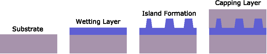
Epitaxy is a crystal growth technique, where the deposited material forms around and continues the underlying crystal order. The term ‘Epitaxy’ comes from the Ancient Greek words epĭ́ and tắxĭs which mean upon or surface, and arrangement or ordering, respectively. The thin, single-crystal layer grown on a crystalline substrate is referred to as the epilayer. The epilayer’s crystal structure and orientation are determined by the substrate, ensuring a high-quality, defect-free layer (known as an epitaxial layer).
What is the difference between epitaxy and device fabrication?
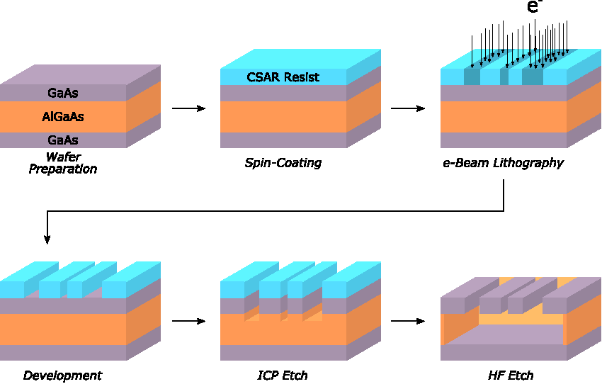
Epitaxy is a process of growing thin, crystalline layers on a substrate, whereas device fabrication is a broader term used for processes such as patterning, depositing metal contacts and cleaving whole wafers into individual components to create functional devices from the epitaxially grown wafers. The wafers need to be fabricated into devices using a range of (electron-beam, photo), lithography, (wet/dry) etching, and deposition methods (evaporation/sputtering).
What materials and structures are you capable of growing?
We provide a full range of group III-V semiconductors and Si/Ge-based group IV materials by both the MBE and MOVPE techniques.
- Group III-V material:
- MOVPE (Sheffield): gallium, aluminium, indium, arsenic, phosphorus plus silicon and tellurium n-dopants and zinc and carbon p-dopants. Both lattice matched and strained combinations are available. We are currently developing capability for antimonides by MOVPE with a view to this being available to the semiconductor research community in the near future.
- MBE (Sheffield): arsenides, phosphides, antimonides, dilute nitrides and dilute bismide epitaxial structures plus silicon and tellurium for n-dopants and beryllium and carbon for p-dopants.
- MOVPE (Cambridge) – Gallium Nitride epitaxy including GaN, AlN, InGaN, AlGaN, AlInN and InAlGaN
- Group IV material:
- MBE (UCL): Silicon and Germanium
What structures and devices can be grown?
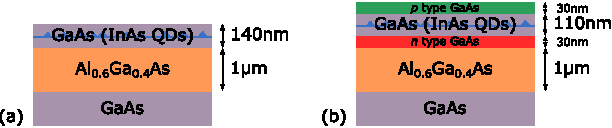
Structures and devices grown include site-controlled quantum dots, single photon avalanche photodiodes (SPADs), LEDs, VCSELs, QCLs, HEMTs, photonic crystal devices, microcavities, and nanowires.
How can I access the Facility?
The National Epitaxy Facility offers wafer design advice and growth. We support researchers applying for funding, those with active grants, and those working in industry/spin-outs.
If you can, please fill out our epitaxy spreadsheet and send it to epitaxyfacility@sheffield.ac.uk to enquire about Facility access. Otherwise please get in touch to arrange a discussion with the epitaxy team to identify your requirements.
When should I contact the Facility to obtain epitaxial wafers in support of my grant?
During the process of writing your grant proposal to allow a full discussion of your requirements and to ensure that the grant budget includes the required epitaxy costs.
What is the Pump Priming scheme?
Our Pump Priming Scheme offers a limited number of wafers free of charge to researchers and without the need for an EPSRC grant. The scheme is designed to stimulate UK strategic activity in III-V and group IV semiconductors with the expectation that the recipient will, within 6 months, write a full EPSRC proposal building on the results of the feasibility study.
Each request will be considered for approval by the National Epitaxy Facility Pump Priming Committee with the selection of projects based on scientific quality, strategic need, and the Facility capability.
Please visit our Pump Priming page for more information.
I am interested in applying to your Pump Priming scheme. When will the next call open?
Pump Priming call usually takes place twice a year. They are advertised on our website, social media and newsletter. Please follow us on social media and sign up to our newsletter, and visit our Pump Priming page for more information.
What size wafers can you grow?
- MOVPE at Sheffield – 2”, 3” and 4”
- MBE at Sheffield – 2, 3 and 4” substrates
- MOVPE at Cambridge – 6” GaN on Si wafers and 2″, 6″, and 8″ Si/Sapphire/SiC substrates
- MBE at UCL – 2” and 3” wafers
What Characterisation equipment do you have?
The Facility in Sheffield has extensive characterisation and device fabrication processing equipment. Structural characterization equipment available includes SEMs, AFMs, XRDs, and microscopes. Electrical techniques used are eCV, IV, and Hall with variable field and temperature. Optical methods include room and low temperature PL and uPL, with a new wafer-scale cryostat.
Structural characterisation equipment in Cambridge includes Electron microscopy, a High-Resolution XRD, Dual-Beam FIB/SEM and Time-resolved Cathodoluminescence Microscopy. Optical characterisation includes a Photoluminescence mapper and electrical characterisation include Variable temperature Hall measurements, Mercury probe C-V measurements and a Probe station.
UCL facilities include an optical characterisation photoluminescence mapper and structural characterisation methods MRD, AFM and SEM.
Do you offer a semiconductor material characterization as a service?
Not normally. We use material characterization to qualify the epitaxial wafers grown for our users as part of our ISO9001 Quality Management process.
Are there facilities for Atomic Layer Deposition (ALD) at the NEF?
At present we don’t have ALD capability. However there is a system being set up by the LDSD group at the University of Sheffield.
Can access to the Micro-Transfer Printing (MTP) system be costed into grants?
It is possible to cost the use of our MTP system on a grant. We will need to know what devices/materials you want to transfer-print, including their sizes to understand whether it is achievable with our system in the first instance. If it is, we can then discuss arrangements for any development work required, as at the moment we do not offer sacrificial membrane development for specific projects.
Do you supply epitaxial structures to research institutes outside the UK?
Generally, we can supply epitaxial structures to researchers outside the UK, however, it is increasingly more difficult due to the new UK export control regulations. Please do get in touch with us describing the materials and structures you are interested in and the country to which the wafers would be supplied to and we can advise you further.
Can I access your EBL and SEM?
Yes, please contact Paul Fry at p.w.fry@sheffield.ac.uk to discuss your requirements.
Do you offer device fabrication as a service?
The National Epitaxy Facility doesn’t offer device fabrication as a service, but the University of Sheffield has these capabilities at the School of Electrical and Electronic Engineering. Please contact Fasihullah Khan at fasihullah.khan@sheffield.ac.uk to discuss your requirements.
Do you offer a commercial epitaxy service?
Yes we have the capability for this. We will ask you to fill out our epitaxy spreadsheet and then provide you with a quotation for the work.
Do you offer metal oxide deposition?
Not currently, but the new double-chamber MBE system due to be installed in the summer of 2026 will have this capability.