January 2026
Gallium nitride is very widely used in blue light emitting diodes (LEDs) and laser diodes (LDs). The blue nitride LED, in particular, lies at the heart of energy efficient solid state lighting, a technology which is transforming the way we light up our world. Now, potential applications of this important optoelectronic material are expanding into the realm of quantum technology. Single photon sources are a key building block in many quantum systems, with potential use cases in quantum computation and quantum key distribution. They can also be used in conventional computation to overcome challenges such as true random number generation. However, generating single photons at room temperature remains a challenging problem. Devices based on quantum dots are often only operational at cryogenic temperature. Meanwhile, colour centres – defects in crystals on the scale of a single atom – may emit single photons at room temperature, but have been most commonly explored in materials like diamond, which do not have the mature device fabrication and manufacturing routes offered by semiconductors.
Colour centres in gallium nitride may offer both room temperature performance and integration with semiconductor processing technologies. The existence of single photon emitting defects in the nitrides has been known since around 2017[1]. These defects have a number of very promising properties including: the availability of emission wavelengths in the ultraviolet, visible, and telecom spectral ranges; excellent temperature stability; and extremely narrow emission linewidths[2]. Unfortunately, the exact nature of the light emitting defect has remained obscure[3], and until recently, there was no available method to control the defect position within a device, rendering development of integrated systems impossible.
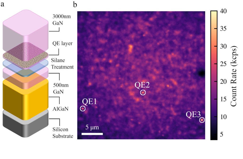
Figure 1: a. Epitaxial structure yielding quantum emitters at a controlled depth in GaN-on-Si epitaxy. b. confocal fluorescence scan map of sample showing quantum emitter (QE) locations.
However, a recent collaboration between the NEF nitride growth activity at Cambridge and the group of Professor Anthony Bennett at Cardiff University has changed all that[4]. Together, the collaborators first showed that in standard GaN epitaxy grown on sapphire, the single photon emitters were located directly at the interface between GaN and sapphire. This is not a favourable location for device integration. However, the NEF growers were able to develop a new growth method that mimicked what occurs during the initial seeding of GaN on sapphire part way through the growth of a nitride layer. They were hence able to achieve the growth of single photon emitters at a controlled depth in a GaN layer, suitable for the growth of subsequent device structures. Not only that, they also transferred the single photon emitter fabrication route to silicon substrates (see Figure 1), offering maximum compatibility with large scale manufacturing routes. State of the art characterisation approaches at Cardiff confirmed the position and properties of the new single photon emitters.
Overall, this research holds great promise for future exploitation of nitride-based colour centres in integrated quantum photonics. The future looks bright for light emitting defects!
References
[1] Berhane et al. Adv. Mater. 2017, 29, 1605092
[2] Kianiniaet al. Optica 2018, 5, 932
[3] Nguyen et al. APL Mater. 2019, 7, 081106
[4] Eggleton et al. APL Photonics 2025, In Press.