Molecular Beam Epitaxy (MBE)
University of Sheffield
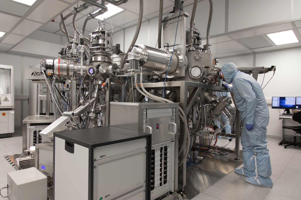
There are three MBE growth systems each of which is operated in a state-of-the-art cleanroom facility based in the Nanosciences & Technology complex at the University of Sheffield – two VG V90 machines and a new dual chamber MBE cluster tool reactor complete with comprehensive in-situ atomic hydrogen cleaning and secondary ion mass spectrometry (SIMS) characterisation capability.
Combined, these three systems allow us to deliver the full range of III-V semiconductor material systems including arsenides, phosphides, antimonides, dilute nitrides and dilute bismide epitaxial structures on 2, 3 and 4” substrates.
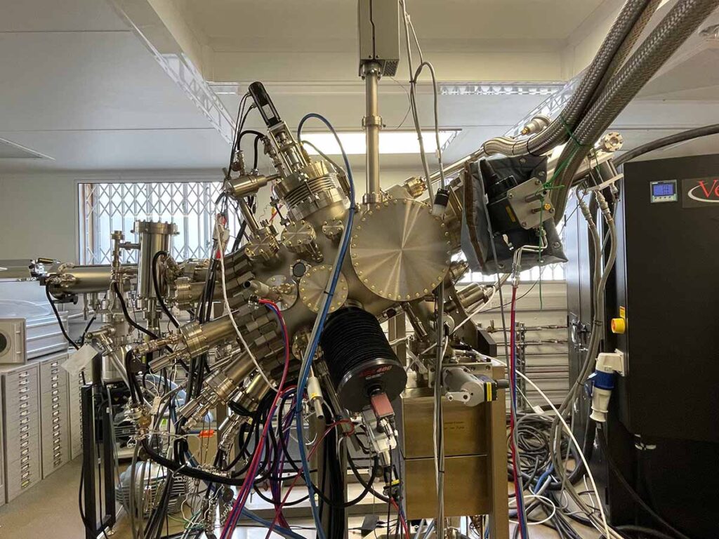
VG Semicon V90-1
- In operation since 2002
- As/P/Bi (or dilute N)
- 12 ports (2x Ga, 2x Al, 2x In, Si, Be, C)
- Wafer size up to 4″/3″/3 x 2″
Application areas:
- Lasers/VCSELs
- Microcavities
- Telecoms-wavelength quantum dots
- QCLs
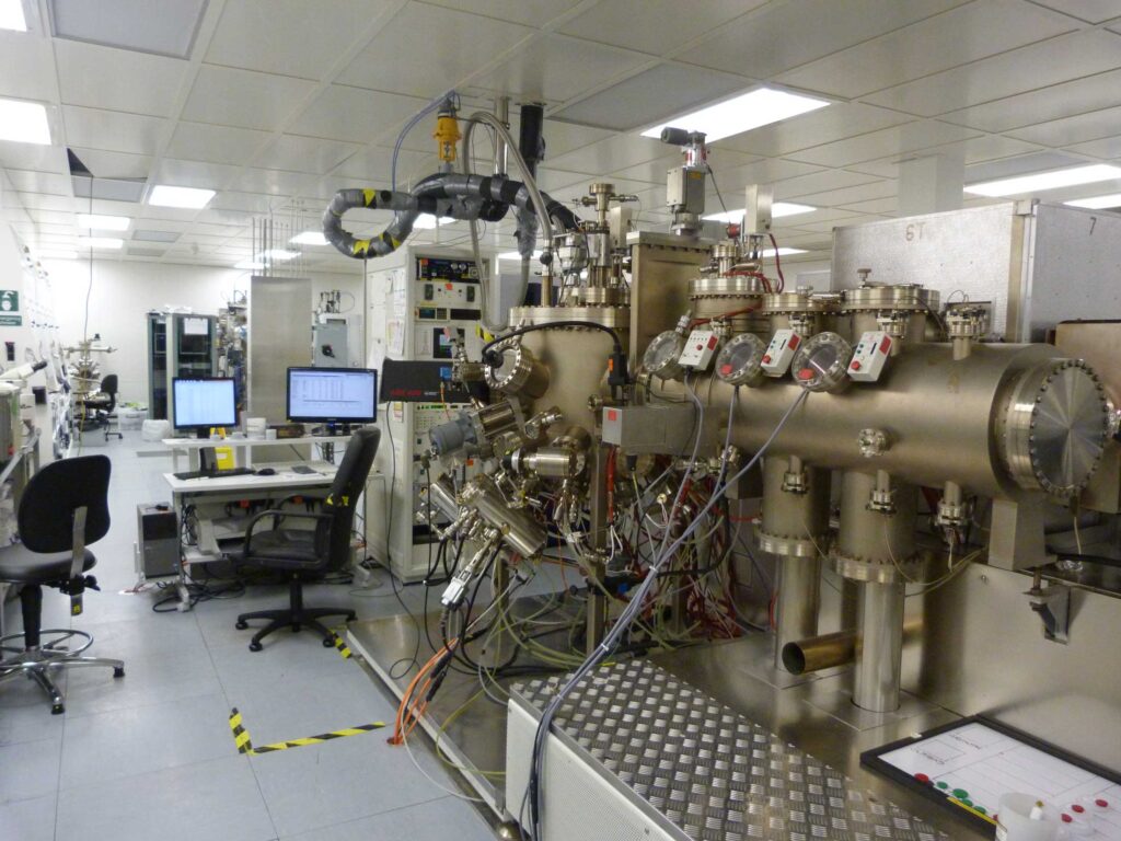
VG Semicon V90-2
- In operation since 2011 (built in 2003)
- As/Sb/Bi
- 10 ports (1x Ga, 1x Al, 2x In, Si, Be, GaTe)
- Wafer size up to 4″ / 3 x 2″
Application areas:
- Mid-IR sources and detectors
- ICLs, QCLs
- APDs
- Type-II Superlattices
- InSb 2DEGs
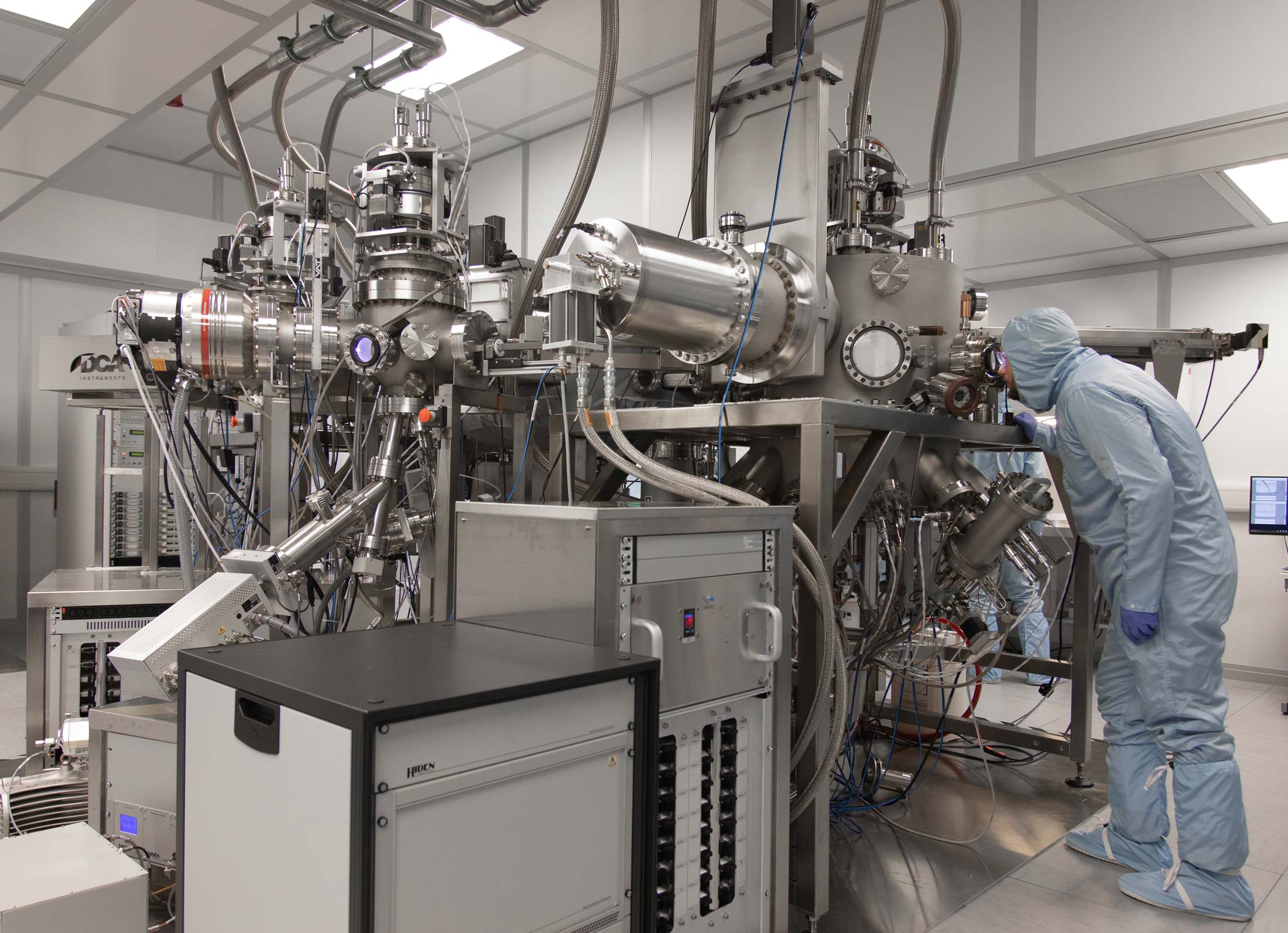
DCA Cluster Tool
- In operation since 2017
- Arsenides only
- Automated sample transfer
- Hydrogen cleaning and SIMS
- Wafer size up to 3″
Application areas:
- Quantum well and quantum dot microcavities
- Waveguide-integrated quantum dot single photon sources
- Site-controlled quantum dots
University College London
The Facility at UCL expanded from the provision of III-V materials and devices to include group IV epitaxy and hybrid III-V/Group IV epitaxy enabling capabilities in, for example, silicon photonics. They have developed growth techniques to enable a wide range of devices using III-V semi-conductors on silicon, such as InAs Quantum Dot lasers, infrared photodetectors and nanowires all grown directly on silicon substrates.
NEF at UCL has two Veeco GEN-930 MBE reactors, one of which has two chambers connected via UHV transfer system for growth of III-Vs on Si/Ge. The Facility can supply large area Silicon and Silicon/Germanium wafers up to 6″ by arrangement.

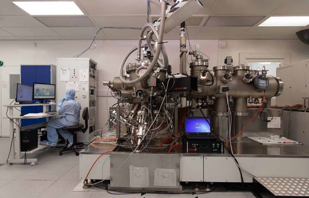
Veeco GEN 930 Twin Chamber System
The twin chamber system enables growth in group IV (Si, Ge) and group III-V (GaAs, InP) materials, without exposing the wafer to the laboratory environment.
- The ability to maintain and transfer wafers under high vacuum from one chamber to the other, ensures the growth surfaces are kept in an ultra-pristine state. Leading to a very low number defects propagating through the growth structure, which in turn results in high quality, high performance devices.
Veeco GEN 930 III-V MBE System
High quality III-V materials growth on Si for a range of projects has been developed on this machine, including:
- III-V quantum dots lasers
- self-catalysed nanowires on Si
- high performance InP based uni-travelling carrier photodiodes and
- GaAs based HEMTs.