
Structural
Sheffield
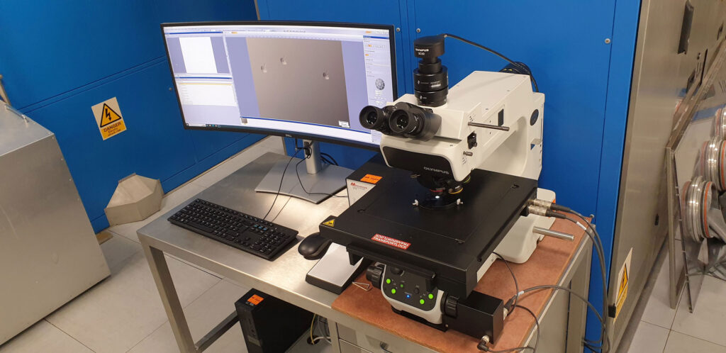
3 microscopes with up to 100x magnification
- Including Olympus Nomarski Optical Microscope for determining surface morphology and defect density
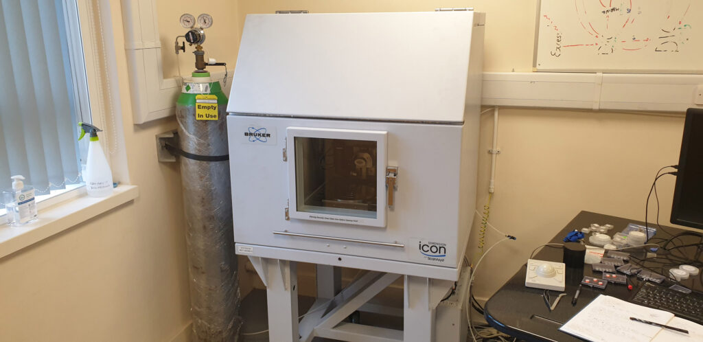
2 AFMs with batch scanning
- Capability for up to 6” / multiple wafers for precise nanoscale imaging for sample surface morphology
- Bruker Dimension ICON AFM
- Veeco Dimension V AFM
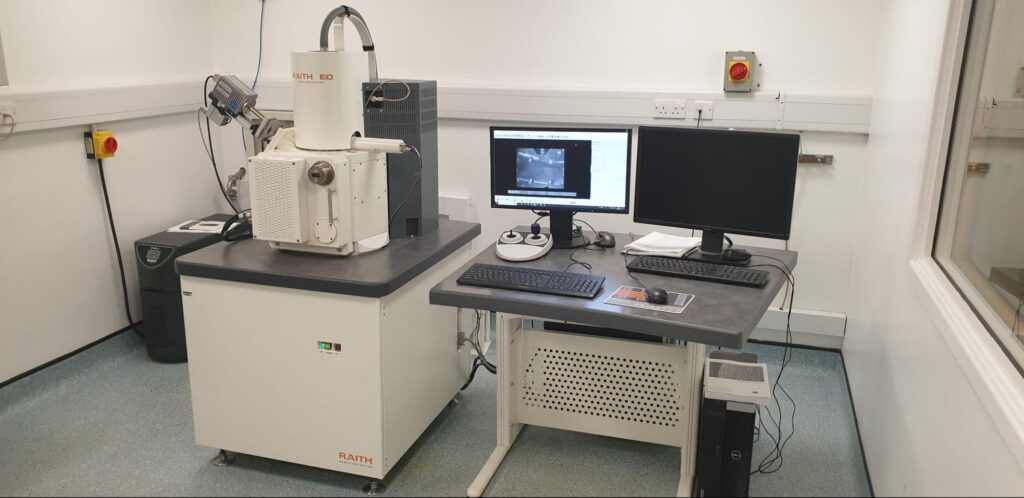
Carl Zeiss FEG SEM with <5nm resolution & EDX
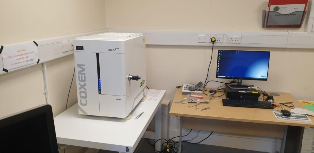
Coxem table top SEM for rapid sample feedback

Bruker & Panalytical XRD Systems
- Up to 6” wafers, used for measuring strain and composition of epitaxy materials
Cambridge
Facilities at Cambridge concentrate on the growth of Gallium Nitride based materials using state of the art electron microscopy and X-ray diffraction facilities.
High-Resolution XRD:
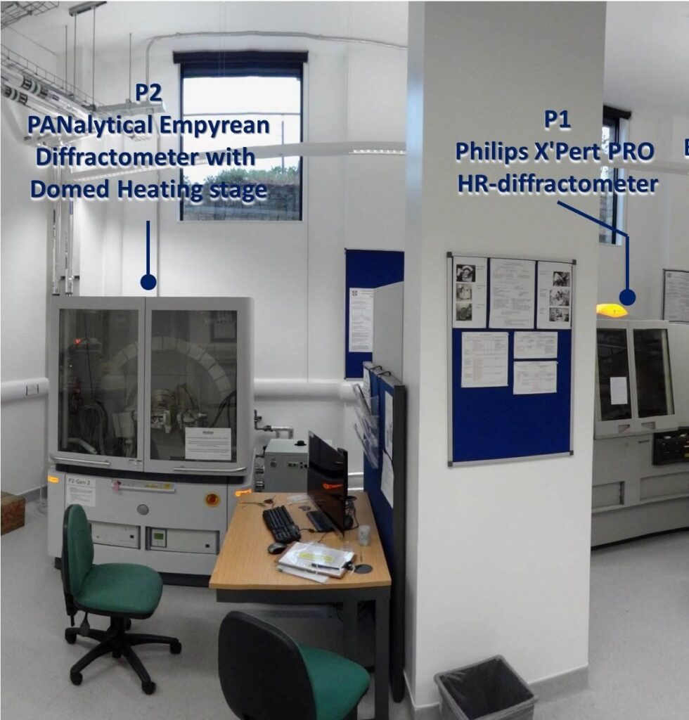
- Philips (PANalytical) high-resolution MRD X-ray diffractometer (P2)
- PANalytical Empyrean diffractometer with PIXcel3D detector (P1)
Electron Microscopy:
- Access to a range of state-of-the art TEM and SEM instruments
- A variable temperature cathodoluminescence (CL) system, which operates in conjunction with an advanced scanning electron microscope (SEM).
- Bruker Dimension ICON AFM
- Veeco Dimension V AFM
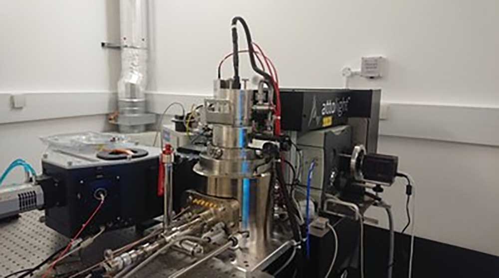
Time-resolved Cathodoluminescence Microscopy (TRCL):
- An Allalin 4027 Chronos from Attolight, designed to work both in continuous (CW) and time-resolved (TR) cathodoluminescence modes.
For more information on the Cambridge characterisation facilities, please visit the Cambridge Centre for Gallium Nitride’s website: https://www.gan.msm.cam.ac.uk/facilities
UCL
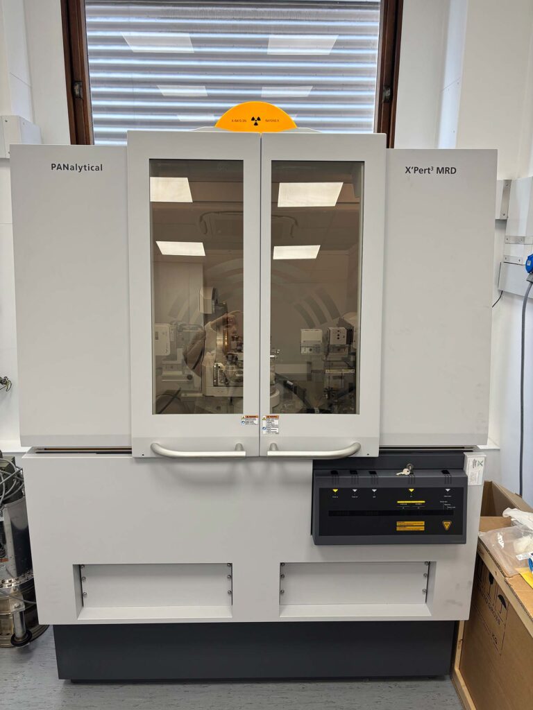
Malvern PANalytical X’Pert3 Materials Research Diffractometer (MRD)
- Fully automated source optics for rapid measurements and switching between different modes
- Complete wafer mapping up to 100 mm is possible.
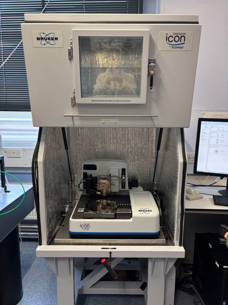
Bruker Dimension Icon AFM
- A maximum scan range of 90 × 90 μm and sub-nanometre height resolution
- Multiple operational modes enabling non-destructive and comprehensive analysis of mechanical, electrical, and magnetic properties.
- Accommodates large samples and offers environmental control options for versatile experimental setups
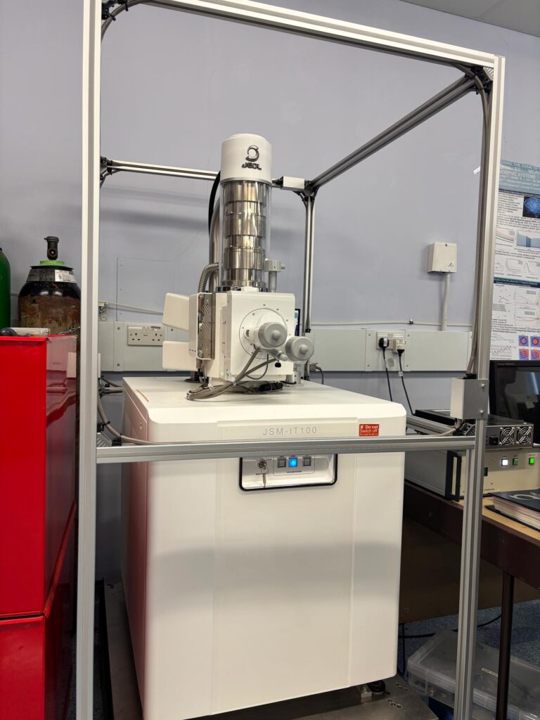
JEOL JSM-IT100 SEM
- Supports high- and low-vacuum operation, enabling the examination of both conductive and non-conductive samples without extensive preparation
- Equipped with a high-sensitivity Everhart-Thornley secondary electron detector (SE) and backscattered electron detector (BSE)
- Accommodates a variety of sample sizes, making it ideal for materials research, failure analysis, and quality control applications.