About Semiconductors
What are semiconductors?
A semiconductor is a material that has electrical conductivity between a conductor and an insulator. Their conductivity can be controlled by adding impurities in a process called doping or by applying electrical fields, light, or heat.
It allows electricity to flow through more easily when the temperature increases, and is used for making electronic devices.

What semiconductor materials are typically used?
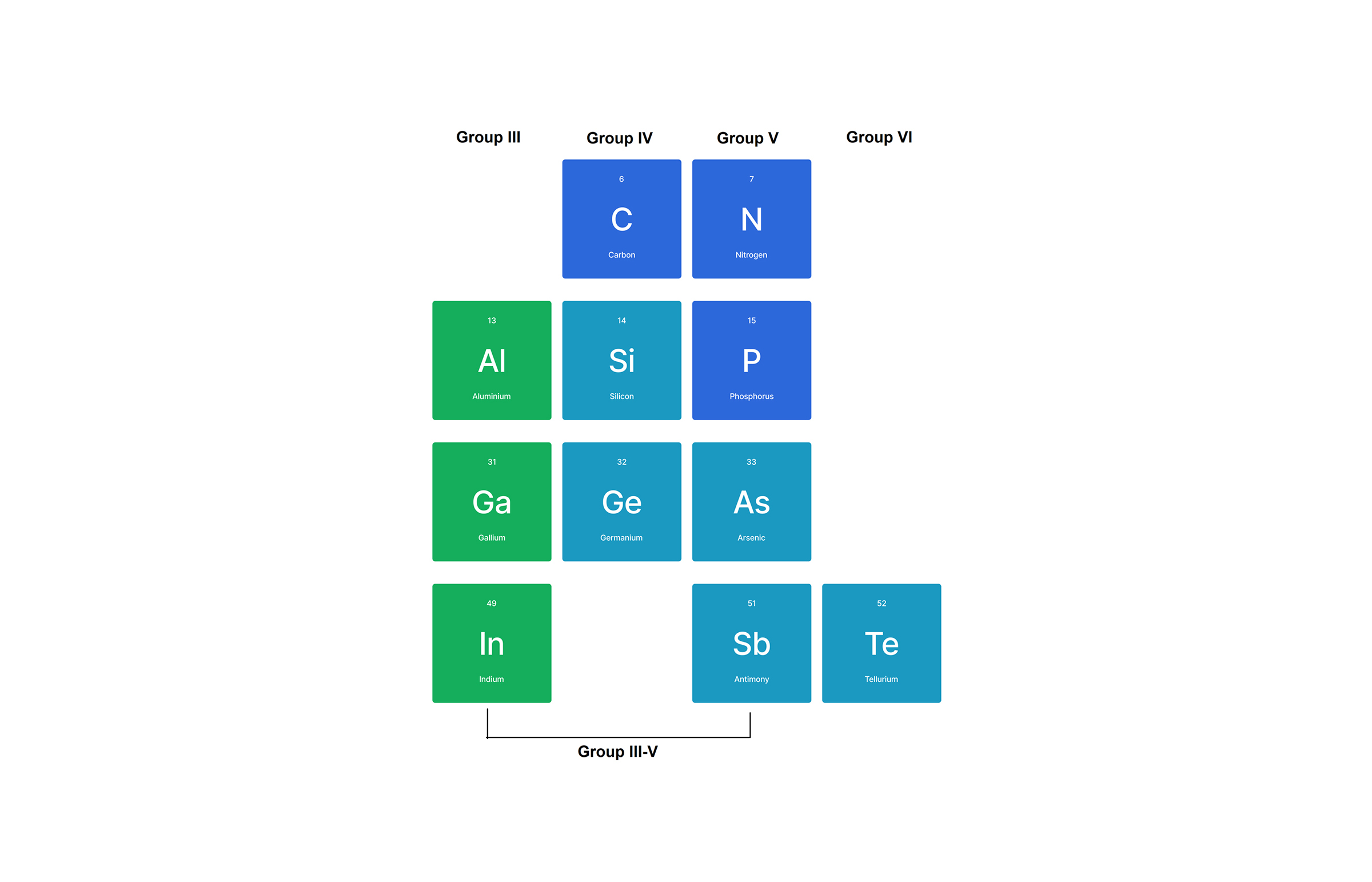
Silicon (Si) and germanium (Ge) are the most commonly used elemental semiconductors. Compound semiconductors use two or more different materials such as Gallium Arsenide (GaAs), Gallium Nitride (GaN), Silicon Carbide (SiC), Cadmium Telluride (CdTe) and Indium Phosphide (InP). And other emerging semiconductor materials are as follows: Graphene, Molybdenum Disulfide (MoS₂), Perovskites.
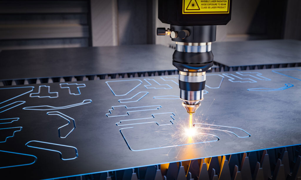
What is a wafer?
A semiconductor wafer is a precisely engineered, thin, circular slice of single-crystal semiconductor material, primarily Si, Ge, GaAs, Etc. serving as the fundamental substrate for the fabrication of integrated circuits (ICs), microchips, and other microelectronic devices.
Through a highly controlled manufacturing process, including doping, oxidation, photolithography, etching, and deposition, these wafers enable the development of high-performance electronic systems. As the foundation of modern semiconductor manufacturing, wafers play a pivotal role in advancing next-generation electronics and innovation.
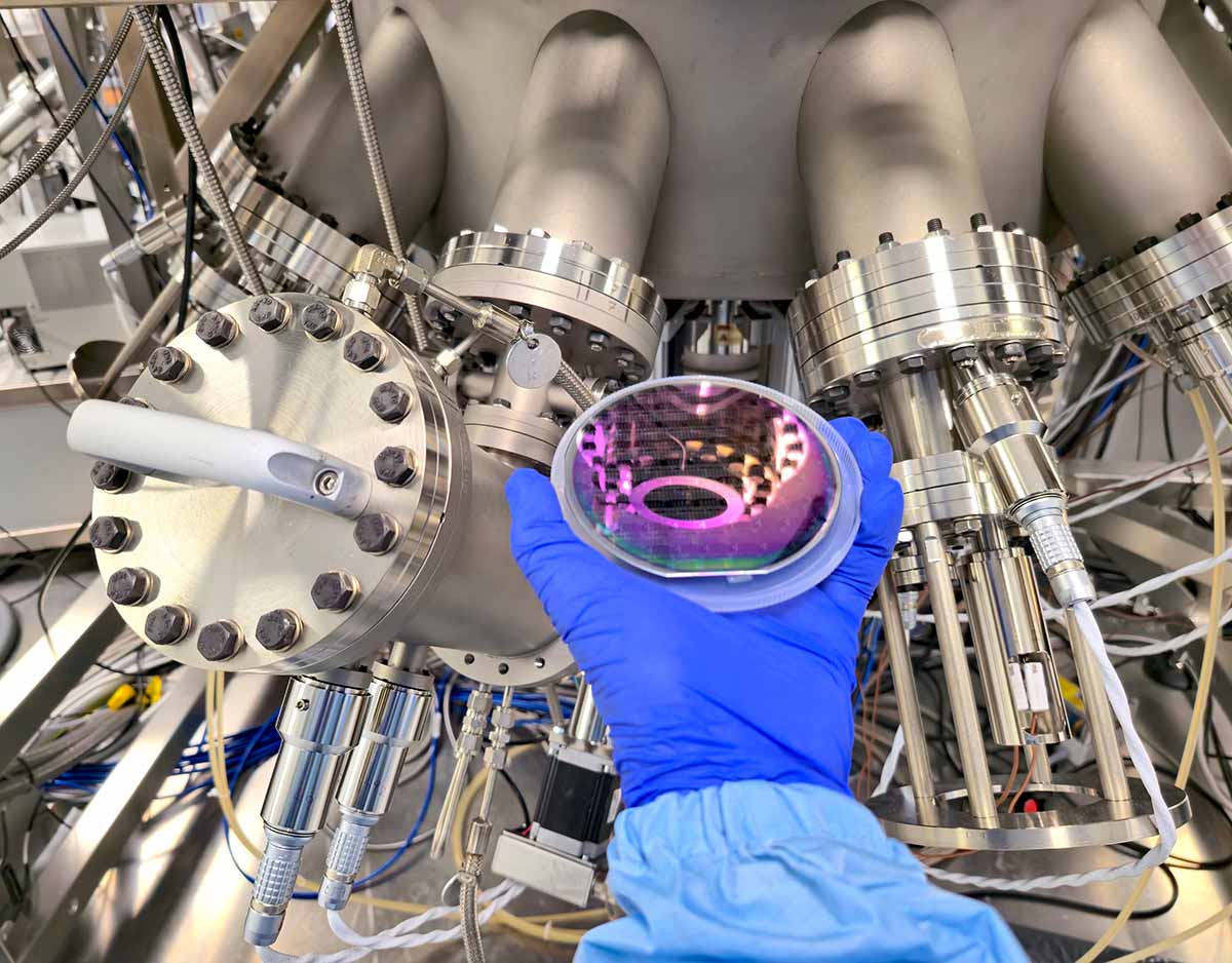
What is MBE?
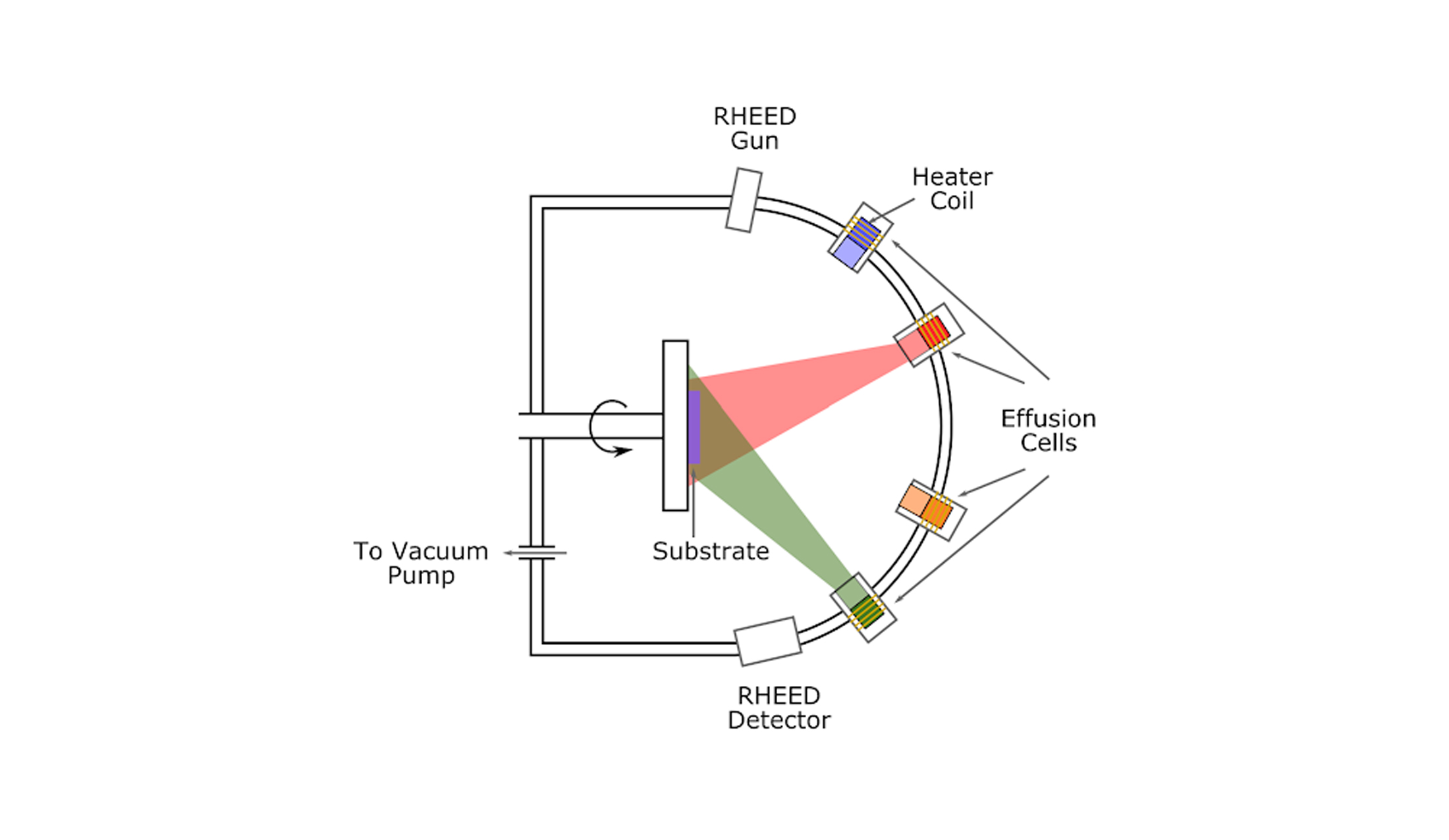
Molecular Beam Epitaxy (MBE) is an advanced thin-film deposition technique used to grow high-purity, ultra-thin layers of crystalline materials, typically semiconductors.
It is a high-vacuum or ultra-high-vacuum (UHV) process that enables precise control over layer thickness, composition, and doping, making it essential for advanced semiconductor devices, optoelectronics, and nanotechnology applications.
What is MOVPE?
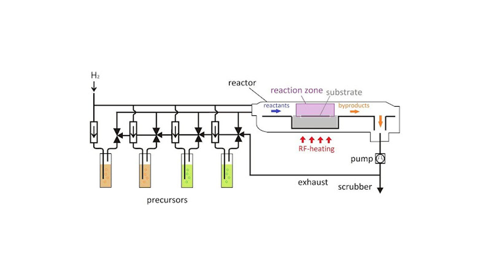
MOVPE stands for Metal Organic Vapour Phase Epitaxy (it is also known as Metal-Organic Chemical Vapour Deposition, MOCVD).
MOVPE uses chemical reactions of metal-organic precursors in a gas-phase environment at low pressure. MOVPE growth rates are generally faster than MBE (0.6 – 4 µm/hr), but require stringent safety mechanisms due to the use of toxic and flammable gases.
What is the difference between MBE and MOVPE?
MBE and NMOVPE are advanced thin-film deposition techniques used for growing high-quality semiconductor layers. However, they differ in their growth mechanisms, operating conditions, and applications. MBE uses physical deposition of atomic or molecular beams under ultra-high vacuum, while MOVPE is a chemical vapor deposition using metal-organic compounds. MBE offers better material purity but is slower, while MOVPE requires more complex infrastructure. Suitability wise MBE is ideal for precision research and specialized applications, whereas MOVPE is the dominant method for industrial-scale semiconductor manufacturing. The choice depends on whether purity and atomic control MBE or high throughput and scalability MOVPE are more critical.
The following are key differences between MBE and MOVPE:
| Feature | Molecular Beam Epitaxy (MBE) | Metal-Organic Vapor Phase Epitaxy (MOVPE/MOCVD) |
|---|---|---|
| Deposition Mechanism | Uses solid elemental sources (e.g., Ga, As, In, Al) heated in effusion cells to produce molecular beams that condense on the substrate. | Uses metal-organic precursors (e.g., Trimethylgallium (TMGa), Trimethylindium (TMIn)) and hydrides (e.g., AsH₃, PH₃) in a chemical reaction that deposits the desired material. |
| Growth Environment | Ultra-High Vacuum (UHV) (10⁻¹⁰ to 10⁻¹² Torr) to prevent contamination and allow precise control. | Atmospheric or low-pressure chamber (10⁻¹ to 10⁻³ Torr) using a controlled gas flow system. |
| Growth Rate | Very slow (typically 1 monolayer per second). | Faster than MBE, making it more efficient for industrial-scale production. |
| Layer Control & Precision | Atomic-level control, making it ideal for superlattices, quantum wells, and nanostructures. | Less precise than MBE, but still allows for high-quality heterostructures. |
| Material Purity | Extremely high purity due to UHV conditions. | Slightly lower purity due to residual gas-phase reactions. |
| Doping Control | Very precise doping control using solid dopants. | More challenging to precisely control doping concentrations. |
| In-Situ Monitoring | Uses Reflection High-Energy Electron Diffraction (RHEED) for real-time monitoring. | Uses optical techniques like in-situ reflectometry and ellipsometry for growth monitoring. |
| Growth Temperature | Low to moderate (400–700°C), reducing thermal damage. | High (600–1200°C), which improves growth efficiency but may induce defects. |
| Scalability | More suited for research and specialized applications due to slow growth. | Industry-preferred for large-scale commercial production. |
| Common Applications | Quantum wells, nanostructures, research-based semiconductor devices. | LED production, high-power and high-frequency electronics, large-scale semiconductor manufacturing. |
What are semiconductors used for?
Semiconductors are the foundation of modern electronics and photonics, used in a wide variety of everyday technology as well as world-class quantum computing research such as:
- Integrated circuits (ICs) or microchips: These are the brains of computers and other electronic devices
- Transistors: These act as electronic switches, controlling the flow of electricity
- Diodes: These allow current to flow in one direction only
- Solar cells: These convert sunlight into electricity
- LEDs (Light Emitting Diodes) and Lasers: These are used for lighting, displays and telecommunications
Why are semiconductors important?
Semiconductors are important because they can be constructed to control the flow of electricity better than other materials, which makes them perfect for many applications. Compound semiconductors are also ideal for converting light into electricity, making them suitable for opto-electronic devices, such as solar cells, lasers, telecommunications, and quantum computing. Semiconductors play a crucial role in shaping the future of technology.
What is the difference between an N-type and P-type semiconductor?
An intrinsic (or undoped) semiconductor will have an equal amount of electrons (negative charge carriers) and holes (vacant electron sites acting as positive charge carriers). By careful substitution of a few group III or V atoms by elements from group II, IV or VI, this balance can be tipped in either direction. N-type semiconductors have an excess of electrons, making the majority charge carrier negative, while P-type semiconductors have an excess of positively charged holes.
Recent developments in semiconductor technology
Recent developments in semiconductors include advancements in AI-accelerated chips, new materials such as Silicon Carbide and Gallium Nitride, and the rise of High-Bandwidth Memory (HBM) for AI workloads, alongside growing focus on advanced packaging and fabrication technologies.
Developments are also pushing towards more stable and scalable quantum computing, such as recent research which has discovered a new quantum state in 2D semiconducting materials that could lead to more reliable data storage in quantum computers.
Examples of semiconductors in everyday life
Semiconductors are the foundation of many electronic and opto-electronic devices such as: