Porous Gallium Nitride
Nitride LEDs are a technology with particularly significant societal impact. Approximately 20% of electricity generated globally is used for lighting, so even small increases in LED efficiency can have a major impact on greenhouse gas emissions, as the use of LED bulbs in domestic and workplace lighting increases. By positioning optical mirrors such as distributed Bragg reflectors (DBRs) on either side of the active region a resonant cavity is formed leading to higher emission intensities, higher spectral purity and more directional emission patterns. The Bragg mirrors are constructed from sub-surface multilayers of alternating materials with high and low refractive index where the optical thicknesses of each layer are close to a quarter of the wavelength of the emitted light in that material.
Challenge
Ideally the Bragg mirrors are made of nitride-based alloys with a high index contrast to maximise the mirror reflectivity AND a minimal lattice mismatch to prevent the generation of cracks in the device structure. Near-lattice matched AlGaN/GaN DBRs achieve an index contrast of ca. 3% [1] while this can be increased to ca. 7% for lattice-matched AlInN/GaN requiring the growth of structures with 20 periods or more to achieve reflectivity of over 90% for application in blue to green light emitting devices [2]. Therefore, the apparent contradiction of optical index contrast and lattice-matching requires a different approach using a DBR design without alloyed nitride layers. The solution lies in a mirror similar to an air-gap DBR using alternating layers of GaN and porous GaN. For instance, a DBR with periodic layers of GaN and 40%-porous GaN achieves an index contrast of 18% while maintaining the near-lattice match.
Solution
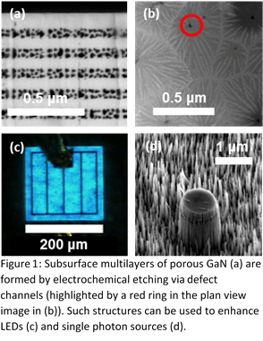
Porosification of GaN epilayers can be achieved using an electrochemical etching process which is sensitive to conductivity. This means the process is selective, since the conductivity of different layers within a multilayer structure can be controlled by changing the concentration of dopants, in particular the n-type conductivity of GaN using Si doping. The first processes developed to fabricate porous GaN required the doped GaN layers to be accessible via a free surface. To porosify multilayer structures it was necessary to dry-etch trenches to allow access to the sub-surface layers [3]. This limited the potential device geometries that could be achieved. However, the Cambridge Centre for Gallium Nitride in association with the National Epitaxy Facility has recently developed and patented [4,5] a novel route for the porosification of sub-surface GaN multilayers (Figure 1(a)), which uses naturally occurring threading dislocations in the GaN crystal (Figure 1(b)) to provide nanoscale channels for vertical etching. The process leaves undoped surface layers almost entirely unaffected, providing an ideal substrate for the overgrowth of further device material. This allows wafer-scale processing and enormous freedom in subsequent device design. The applicability of this process to achieving improved performance in light emitting diodes (LEDs) [64] (Figure 1(c)) and quantum light sources [7] (Figure 1(d)) has been demonstrated.
Conclusion
The future prospects of the porous GaN technology are bright and not only restricted to applications such as DBR mirrors. We have already demonstrated the fabrication of composite materials in which hybrid perovskite materials are incorporated into porous GaN [8]. Hybrid perovskites are an exciting new family of materials which exhibit excellent efficiencies when applied in both solar cells and LEDs. However, their stability is poor, with their properties degrading quickly with time. By encapsulating the porous material in a porous GaN matrix, we were able to extend the life time of its light emitting properties from a few hours to an entire year.
Whilst much work remains to be done to take composites of porous GaN and other functional materials forward to application, these preliminary results are extremely exciting. Nitrides have a range of unusual properties which can allow novel multi-functional materials for sensing, energy harvesting or energy generation to be designed using the composite approach. We are currently pursuing patent protection for a novel porous nitride sensor technology, applicable for sensors operating in high temperature, high radiation dose and/or corrosive environments.
References
[1] D. Brunner, H. Angerer, E. Bustarret, F. Freudenberg, R. Hopler, R. Dimitrov, O. Ambacher, M. Stutzmann, J. Appl. Phys. 82 (1997) 5090
[2] J.-F. Carlin, M. Ilegems, Appl. Phys. Lett., 83 (2003) 668
[3] C. Zhang, S.H. Park, D. Chen, D.-W. Lin, W. Xiong, H.-C. Kuo, C.-F. Lin, H. Cao, J. Han, ACS Photonics 2 (2015) 980
[4] T. Zhu, Y. Liu, T. Ding, W.Y. Fu, J. Jarman, C.X. Ren, R.V. Kumar, R.A. Oliver, Scientific Reports 7 (2017) 45344
[5] Method for Porosifying a Material and Semiconductor Structure. Patent Application Number: PCT/GB2017/052895, Filing Date: 27 September 2017
[6] J.C. Jarman, T. Zhu, P.H. Griffin, R.A. Oliver, Jap. J. Appl. Phys 58 (2019) SCCC14
[7] H.P. Springbett, K. Gao, J. Jarman, T. Zhu, M. Holmes, Y. Arakawa, R.A. Oliver, Appl. Phys. Lett. 113 (2018) 101107
[8] K. T. P. Lim, C. Deakin, B. Ding; X. Bai; P. Griffin, T. Zhu, R.A. Oliver, D. Credgington, APL Mater. 7 (2019) 021107
Download a pdf version:
Case study – Droplet Epitaxy