Silicon-based III-V quantum dot laser
Silicon is the most widely used material for the fabrication of active devices in electronics. However, its indirect band gap structure makes it extremely hard to realise an efficient silicon-based light source. As the speed and complexity of silicon electronics increases, it is becoming harder to interconnect large information processing systems using conventional copper electrical interconnects. There is, thus strongly growing interest in developing optical interconnects for silicon electronics, leading to the research field of silicon photonics.
The ideal light source for silicon photonics would be a semiconductor laser, for high efficiency, direct interfacing with silicon drive electronics and high-speed data modulation capability. To date, the most promising approach to a light source on silicon has been the use of wafer bonding to join direct band gap structure compound semiconductor laser material to a silicon substrate. However, it is very challenging to utilise wafer bonding methods in large-scale, low-cost streamlined device fabrication due to its low yield.
Challenge
Direct epitaxial growth of compound semiconductor laser material on silicon would be a more attractive route to full monolithic integration for silicon photonics. However, the large differences in crystal lattice constant between silicon and compound semiconductors cause dislocations in the crystal structure that have resulted in low efficiency and short operating lifetime for previously demonstrated semiconductor lasers on silicon. Reliable silicon-based laser is of paramount importance to the field of engineering as the area is the core challenge of silicon photonics.
Solution
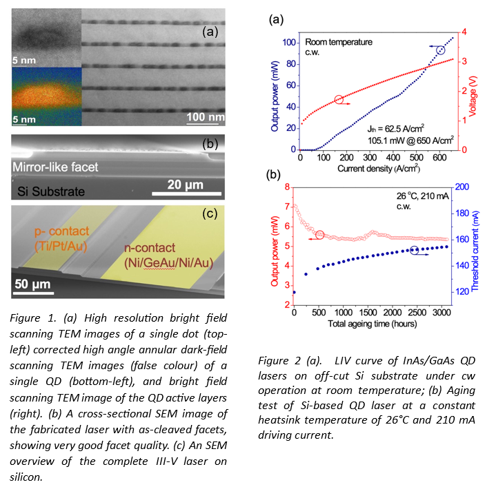
The researchers from the National Epitaxy Facility at UCL first proposed and demonstrated the long lifetime for high-performance semiconductor lasers monolithically grown on silicon platform, by exploiting compound semiconductor quantum-dot materials and devices [1-3], as shown in Figure 1. It has been well established that, lasers with active regions formed from III–V quantum dots — nanosized crystals — can not only offer low threshold current density but can also provide reduced temperature sensitivity [4]. The quantum dots have been further proved by the researchers at the National Epitaxy Facility to be less sensitive to defects than conventional bulk materials and quantum well structures, because carrier localization in quantum dots leads to the reduced interaction with the defect and more efficient carrier capture into quantum dots [1,3,5].
Based on the understanding of the unique properties of III-V quantum dots, the first QD laser on a Ge substrate was demonstrated in 2011 by the researchers at NEF [1]. This work provided a route to direct epitaxial growth on silicon substrates, using commercially available Ge on Si substrates [6]. In 2016, NEF researchers made another breakthrough by demonstrating the first reliable silicon-based laser by monolithic growth [3]. The large lattice mismatch between silicon and GaAs makes this especially challenging. NEF researchers overcame these difficulties by developing special dislocation filtering layers, together with a QD laser gain layer, culminating in the demonstration of an electrically driven 1,300 nm wavelength laser by direct epitaxial growth on silicon. This laser had a low threshold current density of 62.5 A/cm2, a room-temperature output power exceeding 105 mW, lasing operation up to 120 oC, and an extrapolated time to failure of over 100,000 hours, as shown in Figure 2.
Conclusion
Reliable silicon-based laser is of paramount importance to the field of engineering as the area is the core challenge of silicon photonics. There are great difficulties involved in developing the practical silicon-based lasers due to the nature of the group-IV materials and the defect formation of III-V compound semiconductors grown on silicon. The researchers from the National Epitaxy Facility at UCL are the first group that proposed and demonstrated the long-lifetime for high-performance semiconductor lasers monolithically grown on silicon platform, by exploiting compound semiconductor quantum-dot materials and devices. Their works lay the foundation for reliable and cost-effective silicon-based photonic–electronic integration and is of major significance in applications ranging from optical access networks, through data centres to the long-distance optical communication systems.
References
[1] H. Liu et al., Long-wavelength InAs/GaAs quantum-dot laser diode monolithically grown on Ge substrate. Nature Photonics 5, 416-419 (2011)
[2] T. Wang et al., 1.3-?m InAs/GaAs quantum-dot lasers monolithically grown on Si substrates. Opt. Express 19, 11381-11386 (2011)
[3] S. Chen et al., Electrically pumped continuous-wave III-V quantum dot lasers on silicon. Nature Photonics 10, 307-311 (2016)
[4] M. Sugawara and M. Usami, Quantum dot devices: handling the heat. Nature Photonics 3, 30–31 (2009)
[5] Z. Liu et al., Origin of Defect Tolerance in InAs/GaAs Quantum Dot Lasers Grown on Silicon. J. Lightw. Techn. 38, 240-248 (2020)
[6] A. Lee et al., Continuous-wave InAs/GaAs quantum-dot laser diodes monolithically grown on Si substrate with low threshold current densities. Opt. Express 20, 22181-22187 (2012)
Download a pdf version:
Case study – Si-based III-V QD laser