Molecular Beam Epitaxy (MBE)
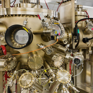
Molecular Beam Epitaxy (MBE) growth in the National Epitaxy Facility is based at the University of Sheffield. The National Epitaxy Facility has three MBE growth systems each of which is operated in a state-of-the-art cleanroom facility based in the Nanosciences & Technology complex at the University of Sheffield; two VG V90 machines and a new dual chamber MBE cluster tool reactor complete with comprehensive in-situ atomic hydrogen cleaning and secondary ion mass spectrometry (SIMS) characterisation capability. Combined, these three systems allow us to deliver the full range of III-V semiconductor material systems including arsenides, phosphides, antimonides, dilute nitrides and dilute bismide epitaxial structures on 2, 3 and 4” substrates.
In support of epitaxy, the Facility also has extensive characterisation and device fabrication processing equipment. Recent investment to our Facility includes XRD, AFM, PL, LT-PL, ICP etcher, ICP-PECVD, O2 asher and rapid thermal annealing.
Structures and devices include:
- GaAs based heterostructures: GaAs, AlGaAs,GalnAs, GalnP
- In based heterostructures: InP, GalnAs, AllnAs, GaAlAsSb
- InAs/GaSb based heterostructures: InAs, GaAlSb, InAsSb
- InGaAs based quantum dots on GaAs and InP
- Dilute nitride: GalnNAs/Bulk, QW and QW lasers
- Quantum cascade lasers QWIP, QDIP structures
- Optoelectronic devices: Lasers, LEDs, photodetectors, APDs, optical modulator, SOA
- Electronic devices: HEMTs, HBT, RTDs
- Bismides
External characterization capabilities include:
- High resolution X-Ray Diffraction (XRD)
- Photoluminescence (PL)
- PL mapping
- Atomic force microscopy (AFM)
- Nomarski optical microscopy
- Hall measurement
- Low temperature PL (LT-PL)
- Micro PL
- Electrochemical capacitance voltage (ECV)
- Scanning electron microscopy (SEM)
- Numerous other techniques provided by carefully selected external collaborators (e.g. SIMS, TEM, XPS, etc.)